Matrox Solios eV-CLBL and eV-CLFL connectors and signal names
This section serves as a reference to match Matrox Solios eV-CLBL's and eV-CLFL's connectors and auxiliary/camera control signals with MIL information, such as MIL auxiliary/camera control signal numbers.
Auxiliary I/O signals and camera control signals can have one or more functionalities (for example, trigger input, timer output, or user output, depending on the signal). Their possible functionalities are described in their description in the pinout table below. Shared input and output signals can be accessed by the digitizers with the specified M_DEV... number. Although a shared signal can be accessed by multiple digitizers, all the functionalities supported by the signal might not be accessible by all these digitizers. In the case of shared output signals, ensure that only one digitizer is driving the output.
Both versions of this board have 4 trigger controllers per acquisition path so that on-board events (for example, acquisition and timer output) can start upon different triggers if required. Although a trigger controller might support several trigger input signals, only one signal can drive a trigger controller at any given time. For example, if you set signal A as the trigger input source for acquisition, and signal B as the trigger input source for timer 1, signal A and B must be driving different trigger controllers; if they drive the same trigger controller, an error is generated. Note that you can set a signal (for example, signal A) as the trigger input source for both acquisition and timer 1; in this case, the associated trigger controller triggers both events at the same time.
Only those auxiliary/camera control signals that have matching MIL information are included in this section. To set/inquire all the settings for this board's auxiliary/camera control signals (for example, signal routing and timer settings), use MdigControl() / MdigInquire(), respectively.
Matrox Solios eV-CLBL has either 2 (if in dual-Base mode) or 1 (if in single-Medium mode) acquisition paths. Matrox Solios eV-CLFL always has 1 acquisition path. For Matrox Solios eV-CLBL and eV-CLFL, only the auxiliary/camera control signals associated with the following device numbers are supported:
|
Matrox Solios eV type |
Device number |
|
Matrox Solios eV-CLBL in dual-Base mode |
|
|
Matrox Solios eV-CLBL in single-Medium mode or eV-CLFL |
The following table lists the different types of configurations possible for the number of acquisition paths available:
|
Digitizer device # |
Matrox Solios eV-CLBL in single-Medium mode or eV-CLFL |
Matrox Solios eV-CLBL in dual-Base mode |
|
Camera Link video input connector 0, External auxiliary I/O connector 0 and 1. |
Camera Link video input connector 0, External auxiliary I/O connector 0 and 1. |
|
|
Camera Link video input connector 1, External auxiliary I/O connector 0 and 1. |
For information on internal connectors and a comprehensive list of all available input and output signals, refer to the board's installation and hardware reference manual.
Board connectors
On the Matrox Solios eV-CLBL and eV-CLFL boards, there are several interface connectors. On its bracket, there are two Camera Link video input connectors. On the DBHD-44/DB-9 cable adapter bracket, there are 2 external auxiliary I/O connectors. On the dual DBHD-15 cable adapter bracket, there are another 2 external auxiliary I/O connectors.
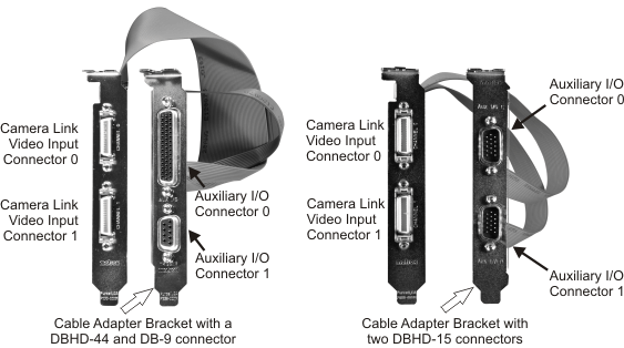
All of Matrox Solios eV-CLBL's and eV-CLFL's connectors have auxiliary/camera control signals with matching MIL information.
|
Connector Name |
Connector Abbreviation |
Image |
Description |
|
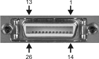
Camera Link video input connectors |
MDR (0 and 1) |
|
The Camera Link video input connectors are 26-pin high-density female connectors. They are used to receive video input, timing, and synchronization signals and transmit/receive communication signals between the video source and the frame grabber. Matrox Solios eV-CLBL and eV-CLFL boards have two Camera Link connectors on their main brackets. |
|
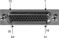
External auxiliary I/O connector 0 |
DBHD-44 or DBHD-15 (0) |
|
External auxiliary I/O connector 0 is used to transmit timing and synchronization signals, and transmit/receive auxiliary signals. Depending on the cable adaptor bracket, external auxiliary I/O connector 0 can be either a high-density D-subminiature 44-pin female connector or a high-density D-subminiature 15-pin male connector. It interfaces with the internal auxiliary I/O connector on the board, making the I/O signals accessible outside the computer enclosure. |
|
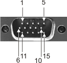
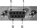
External auxiliary I/O connector 1 |
DB-9 or DBHD-15 (1) |
|
External auxiliary I/O connector 1 is used to transmit/receive auxiliary signals. Depending on the cable adaptor bracket, external auxiliary I/O connector 1 can be either a standard D-subminiature 9-pin female connector or a high-density D-subminiature 15-pin male connector. It interfaces with the internal auxiliary I/O connector on the board, making the I/O signals accessible outside the computer enclosure. |
Signal names and their matching MIL constants
The table below lists the auxiliary/camera control signals with their associated MIL information. Note that the MIL constants in this table are those to use with MIL 10 and later. If you are upgrading from a previous version of MIL, you should port your code using the conversion tables for the Matrox Solios eV-CLBL and eV-CLFL (MILSoliosCameraLinkIOConversionTable ) in the MIL release notes.
  Digitizer device # Digitizer device # |
Description | ||
| MIL I/O # | |||
| Pin information | |||
| Direction | |||
| User-bit information | |||
| Trigger information | |||
| Timer information | |||
| Hardware manual signal name | |||
| Digitizer device #:
M_DEV0 |
Indicates the following. (summarize)Indicates the following. (more details...) |
||
| MIL I/O #: M_AUX_IO0
Shared with: M_DEV1 |
Opto-isolated auxiliary signal (input), shared between both acquisition paths for trigger input or user input, and dedicated to acquisition path 1 for field polarity input. (summarize)Opto-isolated auxiliary signal (input), shared between both acquisition paths for trigger input or user input, and dedicated to acquisition path 1 for field polarity input. (more details...) |
||
| Pin information | Connector: DBHD-44 Pin: 24+,8-; Connector: DBHD-15 (1) Pin: 15+,9- | ||
| Direction |
Input |
||
| Trigger information | Trigger controller: 2 on acq
path 0; 2 or 0 on acq path 1. M_HARDWARE_PORT0; Digitizer device #: M_DEV0, M_DEV1; Trigger controller: 2 on acq path 0; 2 or 0 on acq path 1. |
||
| Hardware manual signal name | OPTO_AUX_IN0 | ||
| MIL I/O #: M_AUX_IO1
Shared with: M_DEV1 |
Opto-isolated auxiliary signal (input), shared between both acquisition paths for trigger input or user input. (summarize)Opto-isolated auxiliary signal (input), shared between both acquisition paths for trigger input or user input. (more details...) |
||
| Pin information | Connector: DBHD-44 Pin: 38+,39-; Connector: DBHD-15 (1) Pin: 12+,11- | ||
| Direction |
Input |
||
| Trigger information | Trigger controller: 3 on acq
path 0; 3 or 1 on acq path 1. M_HARDWARE_PORT1; Digitizer device #: M_DEV0, M_DEV1; Trigger controller: 3 on acq path 0; 3 or 1 on acq path 1. |
||
| Hardware manual signal name | OPTO_AUX_IN1 | ||
| MIL I/O #: M_AUX_IO2
Shared with: M_DEV1 |
TTL auxiliary signal (input/output), shared between both acquisition paths for trigger input, user input, or user output, and dedicated to acquisition path 0 for timer output. (summarize)TTL auxiliary signal (input/output), shared between both acquisition paths for trigger input, user input, or user output, and dedicated to acquisition path 0 for timer output. (more details...) |
||
| Pin information | Connector: DBHD-44 Pin: 43; Connector: DBHD-15 (0) Pin: 3 | ||
| Direction |
Input/Output |
||
| User-bit information |
MIL user-bit #: M_USER_BIT4;
Digitizer device #: M_DEV0,
M_DEV1; (Hardware manual user signal rank 1 : 4 on acq path 0 ; 7 on acq path 1
)
|
||
| Trigger information | Trigger controller: 2 on acq
path 0; 2 on acq path 1. M_HARDWARE_PORT2; Digitizer device #: M_DEV0, M_DEV1; Trigger controller: 2 on acq path 0; 2 on acq path 1. |
||
| Timer information | Timer: M_TIMER2; Digitizer device #: M_DEV0; | ||
| Hardware manual signal name | TTL_AUX_IO_0 | ||
| MIL I/O #: M_AUX_IO3
Shared with: M_DEV1 |
TTL auxiliary signal (input/output), shared between both acquisition paths for trigger input, user input, or user output, and dedicated to acquisition path 1 for timer output. (summarize)TTL auxiliary signal (input/output), shared between both acquisition paths for trigger input, user input, or user output, and dedicated to acquisition path 1 for timer output. (more details...) |
||
| Pin information | Connector: DBHD-44 Pin: 15; Connector: DBHD-15 (1) Pin: 3 | ||
| Direction |
Input/Output |
||
| User-bit information |
MIL user-bit #: M_USER_BIT5;
Digitizer device #: M_DEV0,
M_DEV1; (Hardware manual user signal rank 1 : 7 on acq path 0 ; 4 on acq path 1
)
|
||
| Trigger information | Trigger controller: 3 on acq
path 0; 3 on acq path 1. M_HARDWARE_PORT3; Digitizer device #: M_DEV0, M_DEV1; Trigger controller: 3 on acq path 0; 3 on acq path 1. |
||
| Timer information | Timer: M_TIMER2; Digitizer device #: M_DEV1; | ||
| Hardware manual signal name | TTL_AUX_IO_1 | ||
| MIL I/O #: M_AUX_IO4
Shared with: M_DEV1 |
LVDS auxiliary signal (input), shared between both acquisition paths for trigger input or user input, and dedicated to acquisition path 1 for field polarity input, or quadrature input bit 0. (summarize)LVDS auxiliary signal (input), shared between both acquisition paths for trigger input or user input, and dedicated to acquisition path 1 for field polarity input, or quadrature input bit 0. (more details...) |
||
| Pin information | Connector: DBHD-44 Pin: 32+,31-; Connector: DBHD-15 (1) Pin: 4+,5- | ||
| Direction |
Input |
||
| Trigger information | Trigger controller: 2 on acq
path 0; 2 or 0 on acq path 1. M_HARDWARE_PORT4; Digitizer device #: M_DEV0, M_DEV1; Trigger controller: 2 on acq path 0; 2 or 0 on acq path 1. |
||
| Hardware manual signal name | LVDS_AUX_IN0 | ||
| MIL I/O #: M_AUX_IO5
Shared with: M_DEV1 |
LVDS auxiliary signal (input), shared between both acquisition paths for trigger input or user input, and dedicated to acquisition path 1 for timer clock input or quadrature input bit 1. (summarize)LVDS auxiliary signal (input), shared between both acquisition paths for trigger input or user input, and dedicated to acquisition path 1 for timer clock input or quadrature input bit 1. (more details...) |
||
| Pin information | Connector: DBHD-44 Pin: 12+,28-; Connector: DBHD-15 (1) Pin: 6+,8- | ||
| Direction |
Input |
||
| Trigger information | Trigger controller: 3 on acq
path 0; 3 or 1 on acq path 1. M_HARDWARE_PORT5; Digitizer device #: M_DEV0, M_DEV1; Trigger controller: 3 on acq path 0; 3 or 1 on acq path 1. |
||
| Hardware manual signal name | LVDS_AUX_IN1 | ||
| MIL I/O #: M_AUX_IO6 |
Opto-isolated auxiliary signal (input) for acquisition path 0, which supports: trigger input, user input, or field polarity input. (summarize)Opto-isolated auxiliary signal (input) for acquisition path 0, which supports: trigger input, user input, or field polarity input. (more details...) |
||
| Pin information | Connector: DB-9 Pin: 7+,2-; Connector: DBHD-15 (0) Pin: 15+,9- | ||
| Direction |
Input |
||
| Trigger information | Trigger controller: 0 on acq
path 0. M_HARDWARE_PORT6; Digitizer device #: M_DEV0; Trigger controller: 0 on acq path 0. |
||
| Hardware manual signal name | P0_OPTO_AUX_IN0 | ||
| MIL I/O #: M_AUX_IO7 |
Opto-isolated auxiliary signal (input) for acquisition path 0, which supports: trigger input or user input. (summarize)Opto-isolated auxiliary signal (input) for acquisition path 0, which supports: trigger input or user input. (more details...) |
||
| Pin information | Connector: DB-9 Pin: 4+,5-; Connector: DBHD-15 (0) Pin: 12+,11- | ||
| Direction |
Input |
||
| Trigger information | Trigger controller: 1 on acq
path 0. M_HARDWARE_PORT7; Digitizer device #: M_DEV0; Trigger controller: 1 on acq path 0. |
||
| Hardware manual signal name | P0_OPTO_AUX_IN1 | ||
| MIL I/O #: M_AUX_IO8 |
TTL auxiliary signal (input/output) for acquisition path 0, which supports: timer output, trigger input, user input, user output, or field polarity input. (summarize)TTL auxiliary signal (input/output) for acquisition path 0, which supports: timer output, trigger input, user input, user output, or field polarity input. (more details...) |
||
| Pin information | Connector: DB-9 Pin: 1; Connector: DBHD-15 (0) Pin: 1 | ||
| Direction |
Input/Output |
||
| User-bit information |
MIL user-bit #: M_USER_BIT2;
Digitizer device #: M_DEV0;
(Hardware manual user signal rank 1 : 2 on acq path 0 )
|
||
| Trigger information | Trigger controller: 0 on acq
path 0. M_HARDWARE_PORT8; Digitizer device #: M_DEV0; Trigger controller: 0 on acq path 0. |
||
| Timer information | Timer: M_TIMER3; Digitizer device #: M_DEV0; | ||
| Hardware manual signal name | P0_TTL_AUX_IO_0 | ||
| MIL I/O #: M_AUX_IO9 |
TTL auxiliary signal (input/output) for acquisition path 0, which supports: timer output, trigger input, user input, or user output. (summarize)TTL auxiliary signal (input/output) for acquisition path 0, which supports: timer output, trigger input, user input, or user output. (more details...) |
||
| Pin information | Connector: DBHD-44 Pin: 13; Connector: DBHD-15 (0) Pin: 2 | ||
| Direction |
Input/Output |
||
| User-bit information |
MIL user-bit #: M_USER_BIT3;
Digitizer device #: M_DEV0;
(Hardware manual user signal rank 1 : 3 on acq path 0 )
|
||
| Trigger information | Trigger controller: 1 on acq
path 0. M_HARDWARE_PORT9; Digitizer device #: M_DEV0; Trigger controller: 1 on acq path 0. |
||
| Timer information | Timer: M_TIMER1/M_TIMER4; Digitizer device #: M_DEV0; | ||
| Hardware manual signal name | P0_TTL_AUX_IO_1 | ||
| MIL I/O #: M_AUX_IO10 |
LVDS auxiliary signal (input) for acquisition path 0, which supports: trigger input, user input, field polarity input, or quadrature input bit 0. (summarize)LVDS auxiliary signal (input) for acquisition path 0, which supports: trigger input, user input, field polarity input, or quadrature input bit 0. (more details...) |
||
| Pin information | Connector: DB-9 Pin: 8+,3-; Connector: DBHD-15 (0) Pin: 4+,5- | ||
| Direction |
Input |
||
| Trigger information | Trigger controller: 0 on acq
path 0. M_HARDWARE_PORT10; Digitizer device #: M_DEV0; Trigger controller: 0 on acq path 0. |
||
| Hardware manual signal name | P0_LVDS_AUX_IN0 | ||
| MIL I/O #: M_AUX_IO11 |
LVDS auxiliary signal (input) for acquisition path 0, which supports: trigger input, user input, timer clock input, or quadrature input bit 1. (summarize)LVDS auxiliary signal (input) for acquisition path 0, which supports: trigger input, user input, timer clock input, or quadrature input bit 1. (more details...) |
||
| Pin information | Connector: DBHD-44 Pin: 37+,23-; Connector: DBHD-15 (0) Pin: 6+,8- | ||
| Direction |
Input |
||
| Trigger information | Trigger controller: 1 on acq
path 0. M_HARDWARE_PORT11; Digitizer device #: M_DEV0; Trigger controller: 1 on acq path 0. |
||
| Hardware manual signal name | P0_LVDS_AUX_IN1 | ||
| MIL I/O #: M_AUX_IO12 |
LVDS auxiliary signal (output) for acquisition path 0, which supports: timer output or user output. (summarize)LVDS auxiliary signal (output) for acquisition path 0, which supports: timer output or user output. (more details...) |
||
| Pin information | Connector: DBHD-44 Pin: 20+,4-; Connector: DBHD-15 (0) Pin: 13+,14- | ||
| Direction |
Output |
||
| User-bit information |
MIL user-bit #: M_USER_BIT0;
Digitizer device #: M_DEV0;
(Hardware manual user signal rank 1 : 5 on acq path 0 )
|
||
| Timer information | Timer: M_TIMER1; Digitizer device #: M_DEV0; | ||
| Hardware manual signal name | P0_LVDS_AUX_OUT0 | ||
| MIL I/O #: M_AUX_IO13 |
LVDS auxiliary signal (output) for acquisition path 0, which supports: timer output or user output. (summarize)LVDS auxiliary signal (output) for acquisition path 0, which supports: timer output or user output. (more details...) |
||
| Pin information | Connector: DBHD-44 Pin: 19+,3- | ||
| Direction |
Output |
||
| User-bit information |
MIL user-bit #: M_USER_BIT1;
Digitizer device #: M_DEV0;
(Hardware manual user signal rank 1 : 6 on acq path 0 )
|
||
| Timer information | Timer: M_TIMER2; Digitizer device #: M_DEV0; | ||
| Hardware manual signal name | P0_LVDS_AUX_OUT1 | ||
| MIL I/O #: M_CC_IO1 |
Camera control output 1 for acquisition path 0, which supports: timer output, user output, VSYNC, HSYNC, clock output, or rerouting of specific auxiliary input signals. Only the following auxiliary input signals can be rerouted to this output signal:
Camera control output 1 for acquisition path 0, which supports: timer output, user output, VSYNC, HSYNC, clock output, or rerouting of specific auxiliary input signals. (more details...) |
||
| Pin information | Connector: MDR (0) Pin: 5+,18- | ||
| Direction |
Output |
||
| User-bit information |
MIL user-bit #: M_USER_BIT_CC_IO0/M_USER_BIT_CC_IO1;
Digitizer device #: M_DEV0;
|
||
| Timer information | Timer: M_TIMER1/M_TIMER2; Digitizer device #: M_DEV0; | ||
| Hardware manual signal name | CC1 (0) | ||
| MIL I/O #: M_CC_IO2 |
Camera control output 2 for acquisition path 0, which supports: timer output, user output, VSYNC, HSYNC, clock output, or rerouting of specific auxiliary input signals. Only the following auxiliary input signals can be rerouted to this output signal:
Camera control output 2 for acquisition path 0, which supports: timer output, user output, VSYNC, HSYNC, clock output, or rerouting of specific auxiliary input signals. (more details...) |
||
| Pin information | Connector: MDR (0) Pin: 17+,4- | ||
| Direction |
Output |
||
| User-bit information |
MIL user-bit #: M_USER_BIT_CC_IO0/M_USER_BIT_CC_IO1;
Digitizer device #: M_DEV0;
|
||
| Timer information | Timer: M_TIMER1/M_TIMER2; Digitizer device #: M_DEV0; | ||
| Hardware manual signal name | CC2 (0) | ||
| MIL I/O #: M_CC_IO3 |
Camera control output 3 for acquisition path 0, which supports: timer output, user output, VSYNC, HSYNC, clock output, or rerouting of specific auxiliary input signals. Only the following auxiliary input signals can be rerouted to this output signal:
Camera control output 3 for acquisition path 0, which supports: timer output, user output, VSYNC, HSYNC, clock output, or rerouting of specific auxiliary input signals. (more details...) |
||
| Pin information | Connector: MDR (0) Pin: 3+,16- | ||
| Direction |
Output |
||
| User-bit information |
MIL user-bit #: M_USER_BIT_CC_IO0/M_USER_BIT_CC_IO1;
Digitizer device #: M_DEV0;
|
||
| Timer information | Timer: M_TIMER1/M_TIMER2; Digitizer device #: M_DEV0; | ||
| Hardware manual signal name | CC3 (0) | ||
| MIL I/O #: M_CC_IO4 |
Camera control output 4 for acquisition path 0, which supports: timer output, user output, VSYNC, HSYNC, clock output, or rerouting of specific auxiliary input signals. Only the following auxiliary input signals can be rerouted to this output signal:
Camera control output 4 for acquisition path 0, which supports: timer output, user output, VSYNC, HSYNC, clock output, or rerouting of specific auxiliary input signals. (more details...) |
||
| Pin information | Connector: MDR (0) Pin: 15+,2- | ||
| Direction |
Output |
||
| User-bit information |
MIL user-bit #: M_USER_BIT_CC_IO0/M_USER_BIT_CC_IO1;
Digitizer device #: M_DEV0;
|
||
| Timer information | Timer: M_TIMER1/M_TIMER2; Digitizer device #: M_DEV0; | ||
| Hardware manual signal name | CC4 (0) | ||
| Digitizer device #:
M_DEV1 |
Indicates the following. (summarize)Indicates the following. (more details...) |
||
| MIL I/O #: M_AUX_IO0
Shared with: M_DEV0 |
Opto-isolated auxiliary signal (input), shared between both acquisition paths for trigger input or user input, and dedicated to acquisition path 1 for field polarity input. (summarize)Opto-isolated auxiliary signal (input), shared between both acquisition paths for trigger input or user input, and dedicated to acquisition path 1 for field polarity input. (more details...) |
||
| Pin information | Connector: DBHD-44 Pin: 24+,8-; Connector: DBHD-15 (1) Pin: 15+,9- | ||
| Direction |
Input |
||
| Trigger information | Trigger controller: 2 on acq
path 0; 2 or 0 on acq path 1. M_HARDWARE_PORT0; Digitizer device #: M_DEV0, M_DEV1; Trigger controller: 2 on acq path 0; 2 or 0 on acq path 1. |
||
| Hardware manual signal name | OPTO_AUX_IN0 | ||
| MIL I/O #: M_AUX_IO1
Shared with: M_DEV0 |
Opto-isolated auxiliary signal (input), shared between both acquisition paths for trigger input or user input. (summarize)Opto-isolated auxiliary signal (input), shared between both acquisition paths for trigger input or user input. (more details...) |
||
| Pin information | Connector: DBHD-44 Pin: 38+,39-; Connector: DBHD-15 (1) Pin: 12+,11- | ||
| Direction |
Input |
||
| Trigger information | Trigger controller: 3 on acq
path 0; 3 or 1 on acq path 1. M_HARDWARE_PORT1; Digitizer device #: M_DEV0, M_DEV1; Trigger controller: 3 on acq path 0; 3 or 1 on acq path 1. |
||
| Hardware manual signal name | OPTO_AUX_IN1 | ||
| MIL I/O #: M_AUX_IO2
Shared with: M_DEV0 |
TTL auxiliary signal (input/output), shared between both acquisition paths for trigger input, user input, or user output, and dedicated to acquisition path 0 for timer output. (summarize)TTL auxiliary signal (input/output), shared between both acquisition paths for trigger input, user input, or user output, and dedicated to acquisition path 0 for timer output. (more details...) |
||
| Pin information | Connector: DBHD-44 Pin: 43; Connector: DBHD-15 (0) Pin: 3 | ||
| Direction |
Input/Output |
||
| User-bit information |
MIL user-bit #: M_USER_BIT4;
Digitizer device #: M_DEV0,
M_DEV1; (Hardware manual user signal rank 1 : 4 on acq path 0 ; 7 on acq path 1
)
|
||
| Trigger information | Trigger controller: 2 on acq
path 0; 2 on acq path 1. M_HARDWARE_PORT2; Digitizer device #: M_DEV0, M_DEV1; Trigger controller: 2 on acq path 0; 2 on acq path 1. |
||
| Timer information | Timer: M_TIMER2; Digitizer device #: M_DEV0; | ||
| Hardware manual signal name | TTL_AUX_IO_0 | ||
| MIL I/O #: M_AUX_IO3
Shared with: M_DEV0 |
TTL auxiliary signal (input/output), shared between both acquisition paths for trigger input, user input, or user output, and dedicated to acquisition path 1 for timer output. (summarize)TTL auxiliary signal (input/output), shared between both acquisition paths for trigger input, user input, or user output, and dedicated to acquisition path 1 for timer output. (more details...) |
||
| Pin information | Connector: DBHD-44 Pin: 15; Connector: DBHD-15 (1) Pin: 3 | ||
| Direction |
Input/Output |
||
| User-bit information |
MIL user-bit #: M_USER_BIT5;
Digitizer device #: M_DEV0,
M_DEV1; (Hardware manual user signal rank 1 : 7 on acq path 0 ; 4 on acq path 1
)
|
||
| Trigger information | Trigger controller: 3 on acq
path 0; 3 on acq path 1. M_HARDWARE_PORT3; Digitizer device #: M_DEV0, M_DEV1; Trigger controller: 3 on acq path 0; 3 on acq path 1. |
||
| Timer information | Timer: M_TIMER2; Digitizer device #: M_DEV1; | ||
| Hardware manual signal name | TTL_AUX_IO_1 | ||
| MIL I/O #: M_AUX_IO4
Shared with: M_DEV0 |
LVDS auxiliary signal (input), shared between both acquisition paths for trigger input or user input, and dedicated to acquisition path 1 for field polarity input, or quadrature input bit 0. (summarize)LVDS auxiliary signal (input), shared between both acquisition paths for trigger input or user input, and dedicated to acquisition path 1 for field polarity input, or quadrature input bit 0. (more details...) |
||
| Pin information | Connector: DBHD-44 Pin: 32+,31-; Connector: DBHD-15 (1) Pin: 4+,5- | ||
| Direction |
Input |
||
| Trigger information | Trigger controller: 2 on acq
path 0; 2 or 0 on acq path 1. M_HARDWARE_PORT4; Digitizer device #: M_DEV0, M_DEV1; Trigger controller: 2 on acq path 0; 2 or 0 on acq path 1. |
||
| Hardware manual signal name | LVDS_AUX_IN0 | ||
| MIL I/O #: M_AUX_IO5
Shared with: M_DEV0 |
LVDS auxiliary signal (input), shared between both acquisition paths for trigger input or user input, and dedicated to acquisition path 1 for timer clock input or quadrature input bit 1. (summarize)LVDS auxiliary signal (input), shared between both acquisition paths for trigger input or user input, and dedicated to acquisition path 1 for timer clock input or quadrature input bit 1. (more details...) |
||
| Pin information | Connector: DBHD-44 Pin: 12+,28-; Connector: DBHD-15 (1) Pin: 6+,8- | ||
| Direction |
Input |
||
| Trigger information | Trigger controller: 3 on acq
path 0; 3 or 1 on acq path 1. M_HARDWARE_PORT5; Digitizer device #: M_DEV0, M_DEV1; Trigger controller: 3 on acq path 0; 3 or 1 on acq path 1. |
||
| Hardware manual signal name | LVDS_AUX_IN1 | ||
| MIL I/O #: M_AUX_IO8 |
TTL auxiliary signal (input/output) for acquisition path 1, which supports: timer output, trigger input, user input, user output, or field polarity input. (summarize)TTL auxiliary signal (input/output) for acquisition path 1, which supports: timer output, trigger input, user input, user output, or field polarity input. (more details...) |
||
| Pin information | Connector: DBHD-44 Pin: 35; Connector: DBHD-15 (1) Pin: 1 | ||
| Direction |
Input/Output |
||
| User-bit information |
MIL user-bit #: M_USER_BIT2;
Digitizer device #: M_DEV1;
(Hardware manual user signal rank 1 : 2 on acq path 1 )
|
||
| Trigger information | Trigger controller: 0 on acq
path 1. M_HARDWARE_PORT8; Digitizer device #: M_DEV1; Trigger controller: 0 on acq path 1. |
||
| Timer information | Timer: M_TIMER3; Digitizer device #: M_DEV1; | ||
| Hardware manual signal name | P1_TTL_AUX_IO_0 | ||
| MIL I/O #: M_AUX_IO9 |
TTL auxiliary signal (input/output) for acquisition path 1, which supports: timer output, trigger input, user input, or user output. (summarize)TTL auxiliary signal (input/output) for acquisition path 1, which supports: timer output, trigger input, user input, or user output. (more details...) |
||
| Pin information | Connector: DBHD-44 Pin: 1; Connector: DBHD-15 (1) Pin: 2 | ||
| Direction |
Input/Output |
||
| User-bit information |
MIL user-bit #: M_USER_BIT3;
Digitizer device #: M_DEV1;
(Hardware manual user signal rank 1 : 3 on acq path 1 )
|
||
| Trigger information | Trigger controller: 1 on acq
path 1. M_HARDWARE_PORT9; Digitizer device #: M_DEV1; Trigger controller: 1 on acq path 1. |
||
| Timer information | Timer: M_TIMER1; Digitizer device #: M_DEV1; | ||
| Hardware manual signal name | P1_TTL_AUX_IO_1 | ||
| MIL I/O #: M_AUX_IO12 |
LVDS auxiliary signal (output) for acquisition path 1, which supports: timer output or user output. (summarize)LVDS auxiliary signal (output) for acquisition path 1, which supports: timer output or user output. (more details...) |
||
| Pin information | Connector: DBHD-44 Pin: 33+,18-; Connector: DBHD-15 (1) Pin: 13+,14- | ||
| Direction |
Output |
||
| User-bit information |
MIL user-bit #: M_USER_BIT0;
Digitizer device #: M_DEV1;
(Hardware manual user signal rank 1 : 5 on acq path 1 )
|
||
| Timer information | Timer: M_TIMER1; Digitizer device #: M_DEV1; | ||
| Hardware manual signal name | P1_LVDS_AUX_OUT0 | ||
| MIL I/O #: M_AUX_IO13 |
LVDS auxiliary signal (output) for acquisition path 1, which supports: timer output or user output. (summarize)LVDS auxiliary signal (output) for acquisition path 1, which supports: timer output or user output. (more details...) |
||
| Pin information | Connector: DBHD-44 Pin: 2+,17- | ||
| Direction |
Output |
||
| User-bit information |
MIL user-bit #: M_USER_BIT1;
Digitizer device #: M_DEV1;
(Hardware manual user signal rank 1 : 6 on acq path 1 )
|
||
| Timer information | Timer: M_TIMER2; Digitizer device #: M_DEV1; | ||
| Hardware manual signal name | P1_LVDS_AUX_OUT1 | ||
| MIL I/O #: M_CC_IO1 |
Camera control output 1 for acquisition path 1, which supports: timer output, user output, VSYNC, HSYNC, clock output, or rerouting of specific auxiliary input signals. Only the following auxiliary input signals can be rerouted to this output signal:
Camera control output 1 for acquisition path 1, which supports: timer output, user output, VSYNC, HSYNC, clock output, or rerouting of specific auxiliary input signals. (more details...) |
||
| Pin information | Connector: MDR (1) Pin: 5+,18- | ||
| Direction |
Output |
||
| User-bit information |
MIL user-bit #: M_USER_BIT_CC_IO0/M_USER_BIT_CC_IO1;
Digitizer device #: M_DEV1;
|
||
| Timer information | Timer: M_TIMER1/M_TIMER2; Digitizer device #: M_DEV1; | ||
| Hardware manual signal name | CC1 (1) | ||
| MIL I/O #: M_CC_IO2 |
Camera control output 2 for acquisition path 1, which supports: timer output, user output, VSYNC, HSYNC, clock output, or rerouting of specific auxiliary input signals. Only the following auxiliary input signals can be rerouted to this output signal:
Camera control output 2 for acquisition path 1, which supports: timer output, user output, VSYNC, HSYNC, clock output, or rerouting of specific auxiliary input signals. (more details...) |
||
| Pin information | Connector: MDR (1) Pin: 17+,4- | ||
| Direction |
Output |
||
| User-bit information |
MIL user-bit #: M_USER_BIT_CC_IO0/M_USER_BIT_CC_IO1;
Digitizer device #: M_DEV1;
|
||
| Timer information | Timer: M_TIMER1/M_TIMER2; Digitizer device #: M_DEV1; | ||
| Hardware manual signal name | CC2 (1) | ||
| MIL I/O #: M_CC_IO3 |
Camera control output 3 for acquisition path 1, which supports: timer output, user output, VSYNC, HSYNC, clock output, or rerouting of specific auxiliary input signals. Only the following auxiliary input signals can be rerouted to this output signal:
Camera control output 3 for acquisition path 1, which supports: timer output, user output, VSYNC, HSYNC, clock output, or rerouting of specific auxiliary input signals. (more details...) |
||
| Pin information | Connector: MDR (1) Pin: 3+,16- | ||
| Direction |
Output |
||
| User-bit information |
MIL user-bit #: M_USER_BIT_CC_IO0/M_USER_BIT_CC_IO1;
Digitizer device #: M_DEV1;
|
||
| Timer information | Timer: M_TIMER1/M_TIMER2; Digitizer device #: M_DEV1; | ||
| Hardware manual signal name | CC3 (1) | ||
| MIL I/O #: M_CC_IO4 |
Camera control output 4 for acquisition path 1, which supports: timer output, user output, VSYNC, HSYNC, clock output, or rerouting of specific auxiliary input signals. Only the following auxiliary input signals can be rerouted to this output signal:
Camera control output 4 for acquisition path 1, which supports: timer output, user output, VSYNC, HSYNC, clock output, or rerouting of specific auxiliary input signals. (more details...) |
||
| Pin information | Connector: MDR (1) Pin: 15+,2- | ||
| Direction |
Output |
||
| User-bit information |
MIL user-bit #: M_USER_BIT_CC_IO0/M_USER_BIT_CC_IO1;
Digitizer device #: M_DEV1;
|
||
| Timer information | Timer: M_TIMER1/M_TIMER2; Digitizer device #: M_DEV1; | ||
| Hardware manual signal name | CC4 (1) | ||
|
Digitizer device # |
Description | ||
| MIL I/O # | |||
| Pin information | |||
| Direction | |||
| User-bit information | |||
| Trigger information | |||
| Timer information | |||
| Hardware manual signal name | |||
| Digitizer device #:
M_DEV0 |
Indicates the following. (summarize)Indicates the following. (more details...) |
||
| MIL I/O #: M_AUX_IO0
Shared with: M_DEV1 |
Opto-isolated auxiliary signal (input), shared between both acquisition paths for trigger input or user input, and dedicated to acquisition path 1 for field polarity input. (summarize)Opto-isolated auxiliary signal (input), shared between both acquisition paths for trigger input or user input, and dedicated to acquisition path 1 for field polarity input. (more details...) |
||
| Pin information | Connector: DBHD-44 Pin: 24+,8-; Connector: DBHD-15 (1) Pin: 15+,9- | ||
| Direction |
Input |
||
| Trigger information | Trigger controller: 2 on acq
path 0; 2 or 0 on acq path 1. M_HARDWARE_PORT0; Digitizer device #: M_DEV0, M_DEV1; Trigger controller: 2 on acq path 0; 2 or 0 on acq path 1. |
||
| Hardware manual signal name | OPTO_AUX_IN0 | ||
| MIL I/O #: M_AUX_IO1
Shared with: M_DEV1 |
Opto-isolated auxiliary signal (input), shared between both acquisition paths for trigger input or user input. (summarize)Opto-isolated auxiliary signal (input), shared between both acquisition paths for trigger input or user input. (more details...) |
||
| Pin information | Connector: DBHD-44 Pin: 38+,39-; Connector: DBHD-15 (1) Pin: 12+,11- | ||
| Direction |
Input |
||
| Trigger information | Trigger controller: 3 on acq
path 0; 3 or 1 on acq path 1. M_HARDWARE_PORT1; Digitizer device #: M_DEV0, M_DEV1; Trigger controller: 3 on acq path 0; 3 or 1 on acq path 1. |
||
| Hardware manual signal name | OPTO_AUX_IN1 | ||
| MIL I/O #: M_AUX_IO2
Shared with: M_DEV1 |
TTL auxiliary signal (input/output), shared between both acquisition paths for trigger input, user input, or user output, and dedicated to acquisition path 0 for timer output. (summarize)TTL auxiliary signal (input/output), shared between both acquisition paths for trigger input, user input, or user output, and dedicated to acquisition path 0 for timer output. (more details...) |
||
| Pin information | Connector: DBHD-44 Pin: 43; Connector: DBHD-15 (0) Pin: 3 | ||
| Direction |
Input/Output |
||
| User-bit information |
MIL user-bit #: M_USER_BIT4;
Digitizer device #: M_DEV0,
M_DEV1; (Hardware manual user signal rank 1 : 4 on acq path 0 ; 7 on acq path 1
)
|
||
| Trigger information | Trigger controller: 2 on acq
path 0; 2 on acq path 1. M_HARDWARE_PORT2; Digitizer device #: M_DEV0, M_DEV1; Trigger controller: 2 on acq path 0; 2 on acq path 1. |
||
| Timer information | Timer: M_TIMER2; Digitizer device #: M_DEV0; | ||
| Hardware manual signal name | TTL_AUX_IO_0 | ||
| MIL I/O #: M_AUX_IO3
Shared with: M_DEV1 |
TTL auxiliary signal (input/output), shared between both acquisition paths for trigger input, user input, or user output, and dedicated to acquisition path 1 for timer output. (summarize)TTL auxiliary signal (input/output), shared between both acquisition paths for trigger input, user input, or user output, and dedicated to acquisition path 1 for timer output. (more details...) |
||
| Pin information | Connector: DBHD-44 Pin: 15; Connector: DBHD-15 (1) Pin: 3 | ||
| Direction |
Input/Output |
||
| User-bit information |
MIL user-bit #: M_USER_BIT5;
Digitizer device #: M_DEV0,
M_DEV1; (Hardware manual user signal rank 1 : 7 on acq path 0 ; 4 on acq path 1
)
|
||
| Trigger information | Trigger controller: 3 on acq
path 0; 3 on acq path 1. M_HARDWARE_PORT3; Digitizer device #: M_DEV0, M_DEV1; Trigger controller: 3 on acq path 0; 3 on acq path 1. |
||
| Timer information | Timer: M_TIMER2; Digitizer device #: M_DEV1; | ||
| Hardware manual signal name | TTL_AUX_IO_1 | ||
| MIL I/O #: M_AUX_IO4
Shared with: M_DEV1 |
LVDS auxiliary signal (input), shared between both acquisition paths for trigger input or user input, and dedicated to acquisition path 1 for field polarity input, or quadrature input bit 0. (summarize)LVDS auxiliary signal (input), shared between both acquisition paths for trigger input or user input, and dedicated to acquisition path 1 for field polarity input, or quadrature input bit 0. (more details...) |
||
| Pin information | Connector: DBHD-44 Pin: 32+,31-; Connector: DBHD-15 (1) Pin: 4+,5- | ||
| Direction |
Input |
||
| Trigger information | Trigger controller: 2 on acq
path 0; 2 or 0 on acq path 1. M_HARDWARE_PORT4; Digitizer device #: M_DEV0, M_DEV1; Trigger controller: 2 on acq path 0; 2 or 0 on acq path 1. |
||
| Hardware manual signal name | LVDS_AUX_IN0 | ||
| MIL I/O #: M_AUX_IO5
Shared with: M_DEV1 |
LVDS auxiliary signal (input), shared between both acquisition paths for trigger input or user input, and dedicated to acquisition path 1 for timer clock input or quadrature input bit 1. (summarize)LVDS auxiliary signal (input), shared between both acquisition paths for trigger input or user input, and dedicated to acquisition path 1 for timer clock input or quadrature input bit 1. (more details...) |
||
| Pin information | Connector: DBHD-44 Pin: 12+,28-; Connector: DBHD-15 (1) Pin: 6+,8- | ||
| Direction |
Input |
||
| Trigger information | Trigger controller: 3 on acq
path 0; 3 or 1 on acq path 1. M_HARDWARE_PORT5; Digitizer device #: M_DEV0, M_DEV1; Trigger controller: 3 on acq path 0; 3 or 1 on acq path 1. |
||
| Hardware manual signal name | LVDS_AUX_IN1 | ||
| MIL I/O #: M_AUX_IO6 |
Opto-isolated auxiliary signal (input) for acquisition path 0, which supports: trigger input, user input, or field polarity input. (summarize)Opto-isolated auxiliary signal (input) for acquisition path 0, which supports: trigger input, user input, or field polarity input. (more details...) |
||
| Pin information | Connector: DB-9 Pin: 7+,2-; Connector: DBHD-15 (0) Pin: 15+,9- | ||
| Direction |
Input |
||
| Trigger information | Trigger controller: 0 on acq
path 0. M_HARDWARE_PORT6; Digitizer device #: M_DEV0; Trigger controller: 0 on acq path 0. |
||
| Hardware manual signal name | P0_OPTO_AUX_IN0 | ||
| MIL I/O #: M_AUX_IO7 |
Opto-isolated auxiliary signal (input) for acquisition path 0, which supports: trigger input or user input. (summarize)Opto-isolated auxiliary signal (input) for acquisition path 0, which supports: trigger input or user input. (more details...) |
||
| Pin information | Connector: DB-9 Pin: 4+,5-; Connector: DBHD-15 (0) Pin: 12+,11- | ||
| Direction |
Input |
||
| Trigger information | Trigger controller: 1 on acq
path 0. M_HARDWARE_PORT7; Digitizer device #: M_DEV0; Trigger controller: 1 on acq path 0. |
||
| Hardware manual signal name | P0_OPTO_AUX_IN1 | ||
| MIL I/O #: M_AUX_IO8 |
TTL auxiliary signal (input/output) for acquisition path 0, which supports: timer output, trigger input, user input, user output, or field polarity input. (summarize)TTL auxiliary signal (input/output) for acquisition path 0, which supports: timer output, trigger input, user input, user output, or field polarity input. (more details...) |
||
| Pin information | Connector: DB-9 Pin: 1; Connector: DBHD-15 (0) Pin: 1 | ||
| Direction |
Input/Output |
||
| User-bit information |
MIL user-bit #: M_USER_BIT2;
Digitizer device #: M_DEV0;
(Hardware manual user signal rank 1 : 2 on acq path 0 )
|
||
| Trigger information | Trigger controller: 0 on acq
path 0. M_HARDWARE_PORT8; Digitizer device #: M_DEV0; Trigger controller: 0 on acq path 0. |
||
| Timer information | Timer: M_TIMER3; Digitizer device #: M_DEV0; | ||
| Hardware manual signal name | P0_TTL_AUX_IO_0 | ||
| MIL I/O #: M_AUX_IO9 |
TTL auxiliary signal (input/output) for acquisition path 0, which supports: timer output, trigger input, user input, or user output. (summarize)TTL auxiliary signal (input/output) for acquisition path 0, which supports: timer output, trigger input, user input, or user output. (more details...) |
||
| Pin information | Connector: DBHD-44 Pin: 13; Connector: DBHD-15 (0) Pin: 2 | ||
| Direction |
Input/Output |
||
| User-bit information |
MIL user-bit #: M_USER_BIT3;
Digitizer device #: M_DEV0;
(Hardware manual user signal rank 1 : 3 on acq path 0 )
|
||
| Trigger information | Trigger controller: 1 on acq
path 0. M_HARDWARE_PORT9; Digitizer device #: M_DEV0; Trigger controller: 1 on acq path 0. |
||
| Timer information | Timer: M_TIMER1/M_TIMER4; Digitizer device #: M_DEV0; | ||
| Hardware manual signal name | P0_TTL_AUX_IO_1 | ||
| MIL I/O #: M_AUX_IO10 |
LVDS auxiliary signal (input) for acquisition path 0, which supports: trigger input, user input, field polarity input, or quadrature input bit 0. (summarize)LVDS auxiliary signal (input) for acquisition path 0, which supports: trigger input, user input, field polarity input, or quadrature input bit 0. (more details...) |
||
| Pin information | Connector: DB-9 Pin: 8+,3-; Connector: DBHD-15 (0) Pin: 4+,5- | ||
| Direction |
Input |
||
| Trigger information | Trigger controller: 0 on acq
path 0. M_HARDWARE_PORT10; Digitizer device #: M_DEV0; Trigger controller: 0 on acq path 0. |
||
| Hardware manual signal name | P0_LVDS_AUX_IN0 | ||
| MIL I/O #: M_AUX_IO11 |
LVDS auxiliary signal (input) for acquisition path 0, which supports: trigger input, user input, timer clock input, or quadrature input bit 1. (summarize)LVDS auxiliary signal (input) for acquisition path 0, which supports: trigger input, user input, timer clock input, or quadrature input bit 1. (more details...) |
||
| Pin information | Connector: DBHD-44 Pin: 37+,23-; Connector: DBHD-15 (0) Pin: 6+,8- | ||
| Direction |
Input |
||
| Trigger information | Trigger controller: 1 on acq
path 0. M_HARDWARE_PORT11; Digitizer device #: M_DEV0; Trigger controller: 1 on acq path 0. |
||
| Hardware manual signal name | P0_LVDS_AUX_IN1 | ||
| Digitizer device #:
M_DEV1 |
Indicates the following. (summarize)Indicates the following. (more details...) |
||
| MIL I/O #: M_AUX_IO0
Shared with: M_DEV0 |
Opto-isolated auxiliary signal (input), shared between both acquisition paths for trigger input or user input, and dedicated to acquisition path 1 for field polarity input. (summarize)Opto-isolated auxiliary signal (input), shared between both acquisition paths for trigger input or user input, and dedicated to acquisition path 1 for field polarity input. (more details...) |
||
| Pin information | Connector: DBHD-44 Pin: 24+,8-; Connector: DBHD-15 (1) Pin: 15+,9- | ||
| Direction |
Input |
||
| Trigger information | Trigger controller: 2 on acq
path 0; 2 or 0 on acq path 1. M_HARDWARE_PORT0; Digitizer device #: M_DEV0, M_DEV1; Trigger controller: 2 on acq path 0; 2 or 0 on acq path 1. |
||
| Hardware manual signal name | OPTO_AUX_IN0 | ||
| MIL I/O #: M_AUX_IO1
Shared with: M_DEV0 |
Opto-isolated auxiliary signal (input), shared between both acquisition paths for trigger input or user input. (summarize)Opto-isolated auxiliary signal (input), shared between both acquisition paths for trigger input or user input. (more details...) |
||
| Pin information | Connector: DBHD-44 Pin: 38+,39-; Connector: DBHD-15 (1) Pin: 12+,11- | ||
| Direction |
Input |
||
| Trigger information | Trigger controller: 3 on acq
path 0; 3 or 1 on acq path 1. M_HARDWARE_PORT1; Digitizer device #: M_DEV0, M_DEV1; Trigger controller: 3 on acq path 0; 3 or 1 on acq path 1. |
||
| Hardware manual signal name | OPTO_AUX_IN1 | ||
| MIL I/O #: M_AUX_IO2
Shared with: M_DEV0 |
TTL auxiliary signal (input/output), shared between both acquisition paths for trigger input, user input, or user output, and dedicated to acquisition path 0 for timer output. (summarize)TTL auxiliary signal (input/output), shared between both acquisition paths for trigger input, user input, or user output, and dedicated to acquisition path 0 for timer output. (more details...) |
||
| Pin information | Connector: DBHD-44 Pin: 43; Connector: DBHD-15 (0) Pin: 3 | ||
| Direction |
Input/Output |
||
| User-bit information |
MIL user-bit #: M_USER_BIT4;
Digitizer device #: M_DEV0,
M_DEV1; (Hardware manual user signal rank 1 : 4 on acq path 0 ; 7 on acq path 1
)
|
||
| Trigger information | Trigger controller: 2 on acq
path 0; 2 on acq path 1. M_HARDWARE_PORT2; Digitizer device #: M_DEV0, M_DEV1; Trigger controller: 2 on acq path 0; 2 on acq path 1. |
||
| Timer information | Timer: M_TIMER2; Digitizer device #: M_DEV0; | ||
| Hardware manual signal name | TTL_AUX_IO_0 | ||
| MIL I/O #: M_AUX_IO3
Shared with: M_DEV0 |
TTL auxiliary signal (input/output), shared between both acquisition paths for trigger input, user input, or user output, and dedicated to acquisition path 1 for timer output. (summarize)TTL auxiliary signal (input/output), shared between both acquisition paths for trigger input, user input, or user output, and dedicated to acquisition path 1 for timer output. (more details...) |
||
| Pin information | Connector: DBHD-44 Pin: 15; Connector: DBHD-15 (1) Pin: 3 | ||
| Direction |
Input/Output |
||
| User-bit information |
MIL user-bit #: M_USER_BIT5;
Digitizer device #: M_DEV0,
M_DEV1; (Hardware manual user signal rank 1 : 7 on acq path 0 ; 4 on acq path 1
)
|
||
| Trigger information | Trigger controller: 3 on acq
path 0; 3 on acq path 1. M_HARDWARE_PORT3; Digitizer device #: M_DEV0, M_DEV1; Trigger controller: 3 on acq path 0; 3 on acq path 1. |
||
| Timer information | Timer: M_TIMER2; Digitizer device #: M_DEV1; | ||
| Hardware manual signal name | TTL_AUX_IO_1 | ||
| MIL I/O #: M_AUX_IO4
Shared with: M_DEV0 |
LVDS auxiliary signal (input), shared between both acquisition paths for trigger input or user input, and dedicated to acquisition path 1 for field polarity input, or quadrature input bit 0. (summarize)LVDS auxiliary signal (input), shared between both acquisition paths for trigger input or user input, and dedicated to acquisition path 1 for field polarity input, or quadrature input bit 0. (more details...) |
||
| Pin information | Connector: DBHD-44 Pin: 32+,31-; Connector: DBHD-15 (1) Pin: 4+,5- | ||
| Direction |
Input |
||
| Trigger information | Trigger controller: 2 on acq
path 0; 2 or 0 on acq path 1. M_HARDWARE_PORT4; Digitizer device #: M_DEV0, M_DEV1; Trigger controller: 2 on acq path 0; 2 or 0 on acq path 1. |
||
| Hardware manual signal name | LVDS_AUX_IN0 | ||
| MIL I/O #: M_AUX_IO5
Shared with: M_DEV0 |
LVDS auxiliary signal (input), shared between both acquisition paths for trigger input or user input, and dedicated to acquisition path 1 for timer clock input or quadrature input bit 1. (summarize)LVDS auxiliary signal (input), shared between both acquisition paths for trigger input or user input, and dedicated to acquisition path 1 for timer clock input or quadrature input bit 1. (more details...) |
||
| Pin information | Connector: DBHD-44 Pin: 12+,28-; Connector: DBHD-15 (1) Pin: 6+,8- | ||
| Direction |
Input |
||
| Trigger information | Trigger controller: 3 on acq
path 0; 3 or 1 on acq path 1. M_HARDWARE_PORT5; Digitizer device #: M_DEV0, M_DEV1; Trigger controller: 3 on acq path 0; 3 or 1 on acq path 1. |
||
| Hardware manual signal name | LVDS_AUX_IN1 | ||
| MIL I/O #: M_AUX_IO8 |
TTL auxiliary signal (input/output) for acquisition path 1, which supports: timer output, trigger input, user input, user output, or field polarity input. (summarize)TTL auxiliary signal (input/output) for acquisition path 1, which supports: timer output, trigger input, user input, user output, or field polarity input. (more details...) |
||
| Pin information | Connector: DBHD-44 Pin: 35; Connector: DBHD-15 (1) Pin: 1 | ||
| Direction |
Input/Output |
||
| User-bit information |
MIL user-bit #: M_USER_BIT2;
Digitizer device #: M_DEV1;
(Hardware manual user signal rank 1 : 2 on acq path 1 )
|
||
| Trigger information | Trigger controller: 0 on acq
path 1. M_HARDWARE_PORT8; Digitizer device #: M_DEV1; Trigger controller: 0 on acq path 1. |
||
| Timer information | Timer: M_TIMER3; Digitizer device #: M_DEV1; | ||
| Hardware manual signal name | P1_TTL_AUX_IO_0 | ||
| MIL I/O #: M_AUX_IO9 |
TTL auxiliary signal (input/output) for acquisition path 1, which supports: timer output, trigger input, user input, or user output. (summarize)TTL auxiliary signal (input/output) for acquisition path 1, which supports: timer output, trigger input, user input, or user output. (more details...) |
||
| Pin information | Connector: DBHD-44 Pin: 1; Connector: DBHD-15 (1) Pin: 2 | ||
| Direction |
Input/Output |
||
| User-bit information |
MIL user-bit #: M_USER_BIT3;
Digitizer device #: M_DEV1;
(Hardware manual user signal rank 1 : 3 on acq path 1 )
|
||
| Trigger information | Trigger controller: 1 on acq
path 1. M_HARDWARE_PORT9; Digitizer device #: M_DEV1; Trigger controller: 1 on acq path 1. |
||
| Timer information | Timer: M_TIMER1; Digitizer device #: M_DEV1; | ||
| Hardware manual signal name | P1_TTL_AUX_IO_1 | ||
|
Digitizer device # |
Description | ||
| MIL I/O # | |||
| Pin information | |||
| Direction | |||
| User-bit information | |||
| Trigger information | |||
| Timer information | |||
| Hardware manual signal name | |||
| Digitizer device #:
M_DEV0 |
Indicates the following. (summarize)Indicates the following. (more details...) |
||
| MIL I/O #: M_AUX_IO2
Shared with: M_DEV1 |
TTL auxiliary signal (input/output), shared between both acquisition paths for trigger input, user input, or user output, and dedicated to acquisition path 0 for timer output. (summarize)TTL auxiliary signal (input/output), shared between both acquisition paths for trigger input, user input, or user output, and dedicated to acquisition path 0 for timer output. (more details...) |
||
| Pin information | Connector: DBHD-44 Pin: 43; Connector: DBHD-15 (0) Pin: 3 | ||
| Direction |
Input/Output |
||
| User-bit information |
MIL user-bit #: M_USER_BIT4;
Digitizer device #: M_DEV0,
M_DEV1; (Hardware manual user signal rank 1 : 4 on acq path 0 ; 7 on acq path 1
)
|
||
| Trigger information | Trigger controller: 2 on acq
path 0; 2 on acq path 1. M_HARDWARE_PORT2; Digitizer device #: M_DEV0, M_DEV1; Trigger controller: 2 on acq path 0; 2 on acq path 1. |
||
| Timer information | Timer: M_TIMER2; Digitizer device #: M_DEV0; | ||
| Hardware manual signal name | TTL_AUX_IO_0 | ||
| MIL I/O #: M_AUX_IO3
Shared with: M_DEV1 |
TTL auxiliary signal (input/output), shared between both acquisition paths for trigger input, user input, or user output, and dedicated to acquisition path 1 for timer output. (summarize)TTL auxiliary signal (input/output), shared between both acquisition paths for trigger input, user input, or user output, and dedicated to acquisition path 1 for timer output. (more details...) |
||
| Pin information | Connector: DBHD-44 Pin: 15; Connector: DBHD-15 (1) Pin: 3 | ||
| Direction |
Input/Output |
||
| User-bit information |
MIL user-bit #: M_USER_BIT5;
Digitizer device #: M_DEV0,
M_DEV1; (Hardware manual user signal rank 1 : 7 on acq path 0 ; 4 on acq path 1
)
|
||
| Trigger information | Trigger controller: 3 on acq
path 0; 3 on acq path 1. M_HARDWARE_PORT3; Digitizer device #: M_DEV0, M_DEV1; Trigger controller: 3 on acq path 0; 3 on acq path 1. |
||
| Timer information | Timer: M_TIMER2; Digitizer device #: M_DEV1; | ||
| Hardware manual signal name | TTL_AUX_IO_1 | ||
| MIL I/O #: M_AUX_IO8 |
TTL auxiliary signal (input/output) for acquisition path 0, which supports: timer output, trigger input, user input, user output, or field polarity input. (summarize)TTL auxiliary signal (input/output) for acquisition path 0, which supports: timer output, trigger input, user input, user output, or field polarity input. (more details...) |
||
| Pin information | Connector: DB-9 Pin: 1; Connector: DBHD-15 (0) Pin: 1 | ||
| Direction |
Input/Output |
||
| User-bit information |
MIL user-bit #: M_USER_BIT2;
Digitizer device #: M_DEV0;
(Hardware manual user signal rank 1 : 2 on acq path 0 )
|
||
| Trigger information | Trigger controller: 0 on acq
path 0. M_HARDWARE_PORT8; Digitizer device #: M_DEV0; Trigger controller: 0 on acq path 0. |
||
| Timer information | Timer: M_TIMER3; Digitizer device #: M_DEV0; | ||
| Hardware manual signal name | P0_TTL_AUX_IO_0 | ||
| MIL I/O #: M_AUX_IO9 |
TTL auxiliary signal (input/output) for acquisition path 0, which supports: timer output, trigger input, user input, or user output. (summarize)TTL auxiliary signal (input/output) for acquisition path 0, which supports: timer output, trigger input, user input, or user output. (more details...) |
||
| Pin information | Connector: DBHD-44 Pin: 13; Connector: DBHD-15 (0) Pin: 2 | ||
| Direction |
Input/Output |
||
| User-bit information |
MIL user-bit #: M_USER_BIT3;
Digitizer device #: M_DEV0;
(Hardware manual user signal rank 1 : 3 on acq path 0 )
|
||
| Trigger information | Trigger controller: 1 on acq
path 0. M_HARDWARE_PORT9; Digitizer device #: M_DEV0; Trigger controller: 1 on acq path 0. |
||
| Timer information | Timer: M_TIMER1/M_TIMER4; Digitizer device #: M_DEV0; | ||
| Hardware manual signal name | P0_TTL_AUX_IO_1 | ||
| MIL I/O #: M_AUX_IO12 |
LVDS auxiliary signal (output) for acquisition path 0, which supports: timer output or user output. (summarize)LVDS auxiliary signal (output) for acquisition path 0, which supports: timer output or user output. (more details...) |
||
| Pin information | Connector: DBHD-44 Pin: 20+,4-; Connector: DBHD-15 (0) Pin: 13+,14- | ||
| Direction |
Output |
||
| User-bit information |
MIL user-bit #: M_USER_BIT0;
Digitizer device #: M_DEV0;
(Hardware manual user signal rank 1 : 5 on acq path 0 )
|
||
| Timer information | Timer: M_TIMER1; Digitizer device #: M_DEV0; | ||
| Hardware manual signal name | P0_LVDS_AUX_OUT0 | ||
| MIL I/O #: M_AUX_IO13 |
LVDS auxiliary signal (output) for acquisition path 0, which supports: timer output or user output. (summarize)LVDS auxiliary signal (output) for acquisition path 0, which supports: timer output or user output. (more details...) |
||
| Pin information | Connector: DBHD-44 Pin: 19+,3- | ||
| Direction |
Output |
||
| User-bit information |
MIL user-bit #: M_USER_BIT1;
Digitizer device #: M_DEV0;
(Hardware manual user signal rank 1 : 6 on acq path 0 )
|
||
| Timer information | Timer: M_TIMER2; Digitizer device #: M_DEV0; | ||
| Hardware manual signal name | P0_LVDS_AUX_OUT1 | ||
| MIL I/O #: M_CC_IO1 |
Camera control output 1 for acquisition path 0, which supports: timer output, user output, VSYNC, HSYNC, clock output, or rerouting of specific auxiliary input signals. Only the following auxiliary input signals can be rerouted to this output signal:
Camera control output 1 for acquisition path 0, which supports: timer output, user output, VSYNC, HSYNC, clock output, or rerouting of specific auxiliary input signals. (more details...) |
||
| Pin information | Connector: MDR (0) Pin: 5+,18- | ||
| Direction |
Output |
||
| User-bit information |
MIL user-bit #: M_USER_BIT_CC_IO0/M_USER_BIT_CC_IO1;
Digitizer device #: M_DEV0;
|
||
| Timer information | Timer: M_TIMER1/M_TIMER2; Digitizer device #: M_DEV0; | ||
| Hardware manual signal name | CC1 (0) | ||
| MIL I/O #: M_CC_IO2 |
Camera control output 2 for acquisition path 0, which supports: timer output, user output, VSYNC, HSYNC, clock output, or rerouting of specific auxiliary input signals. Only the following auxiliary input signals can be rerouted to this output signal:
Camera control output 2 for acquisition path 0, which supports: timer output, user output, VSYNC, HSYNC, clock output, or rerouting of specific auxiliary input signals. (more details...) |
||
| Pin information | Connector: MDR (0) Pin: 17+,4- | ||
| Direction |
Output |
||
| User-bit information |
MIL user-bit #: M_USER_BIT_CC_IO0/M_USER_BIT_CC_IO1;
Digitizer device #: M_DEV0;
|
||
| Timer information | Timer: M_TIMER1/M_TIMER2; Digitizer device #: M_DEV0; | ||
| Hardware manual signal name | CC2 (0) | ||
| MIL I/O #: M_CC_IO3 |
Camera control output 3 for acquisition path 0, which supports: timer output, user output, VSYNC, HSYNC, clock output, or rerouting of specific auxiliary input signals. Only the following auxiliary input signals can be rerouted to this output signal:
Camera control output 3 for acquisition path 0, which supports: timer output, user output, VSYNC, HSYNC, clock output, or rerouting of specific auxiliary input signals. (more details...) |
||
| Pin information | Connector: MDR (0) Pin: 3+,16- | ||
| Direction |
Output |
||
| User-bit information |
MIL user-bit #: M_USER_BIT_CC_IO0/M_USER_BIT_CC_IO1;
Digitizer device #: M_DEV0;
|
||
| Timer information | Timer: M_TIMER1/M_TIMER2; Digitizer device #: M_DEV0; | ||
| Hardware manual signal name | CC3 (0) | ||
| MIL I/O #: M_CC_IO4 |
Camera control output 4 for acquisition path 0, which supports: timer output, user output, VSYNC, HSYNC, clock output, or rerouting of specific auxiliary input signals. Only the following auxiliary input signals can be rerouted to this output signal:
Camera control output 4 for acquisition path 0, which supports: timer output, user output, VSYNC, HSYNC, clock output, or rerouting of specific auxiliary input signals. (more details...) |
||
| Pin information | Connector: MDR (0) Pin: 15+,2- | ||
| Direction |
Output |
||
| User-bit information |
MIL user-bit #: M_USER_BIT_CC_IO0/M_USER_BIT_CC_IO1;
Digitizer device #: M_DEV0;
|
||
| Timer information | Timer: M_TIMER1/M_TIMER2; Digitizer device #: M_DEV0; | ||
| Hardware manual signal name | CC4 (0) | ||
| Digitizer device #:
M_DEV1 |
Indicates the following. (summarize)Indicates the following. (more details...) |
||
| MIL I/O #: M_AUX_IO2
Shared with: M_DEV0 |
TTL auxiliary signal (input/output), shared between both acquisition paths for trigger input, user input, or user output, and dedicated to acquisition path 0 for timer output. (summarize)TTL auxiliary signal (input/output), shared between both acquisition paths for trigger input, user input, or user output, and dedicated to acquisition path 0 for timer output. (more details...) |
||
| Pin information | Connector: DBHD-44 Pin: 43; Connector: DBHD-15 (0) Pin: 3 | ||
| Direction |
Input/Output |
||
| User-bit information |
MIL user-bit #: M_USER_BIT4;
Digitizer device #: M_DEV0,
M_DEV1; (Hardware manual user signal rank 1 : 4 on acq path 0 ; 7 on acq path 1
)
|
||
| Trigger information | Trigger controller: 2 on acq
path 0; 2 on acq path 1. M_HARDWARE_PORT2; Digitizer device #: M_DEV0, M_DEV1; Trigger controller: 2 on acq path 0; 2 on acq path 1. |
||
| Timer information | Timer: M_TIMER2; Digitizer device #: M_DEV0; | ||
| Hardware manual signal name | TTL_AUX_IO_0 | ||
| MIL I/O #: M_AUX_IO3
Shared with: M_DEV0 |
TTL auxiliary signal (input/output), shared between both acquisition paths for trigger input, user input, or user output, and dedicated to acquisition path 1 for timer output. (summarize)TTL auxiliary signal (input/output), shared between both acquisition paths for trigger input, user input, or user output, and dedicated to acquisition path 1 for timer output. (more details...) |
||
| Pin information | Connector: DBHD-44 Pin: 15; Connector: DBHD-15 (1) Pin: 3 | ||
| Direction |
Input/Output |
||
| User-bit information |
MIL user-bit #: M_USER_BIT5;
Digitizer device #: M_DEV0,
M_DEV1; (Hardware manual user signal rank 1 : 7 on acq path 0 ; 4 on acq path 1
)
|
||
| Trigger information | Trigger controller: 3 on acq
path 0; 3 on acq path 1. M_HARDWARE_PORT3; Digitizer device #: M_DEV0, M_DEV1; Trigger controller: 3 on acq path 0; 3 on acq path 1. |
||
| Timer information | Timer: M_TIMER2; Digitizer device #: M_DEV1; | ||
| Hardware manual signal name | TTL_AUX_IO_1 | ||
| MIL I/O #: M_AUX_IO8 |
TTL auxiliary signal (input/output) for acquisition path 1, which supports: timer output, trigger input, user input, user output, or field polarity input. (summarize)TTL auxiliary signal (input/output) for acquisition path 1, which supports: timer output, trigger input, user input, user output, or field polarity input. (more details...) |
||
| Pin information | Connector: DBHD-44 Pin: 35; Connector: DBHD-15 (1) Pin: 1 | ||
| Direction |
Input/Output |
||
| User-bit information |
MIL user-bit #: M_USER_BIT2;
Digitizer device #: M_DEV1;
(Hardware manual user signal rank 1 : 2 on acq path 1 )
|
||
| Trigger information | Trigger controller: 0 on acq
path 1. M_HARDWARE_PORT8; Digitizer device #: M_DEV1; Trigger controller: 0 on acq path 1. |
||
| Timer information | Timer: M_TIMER3; Digitizer device #: M_DEV1; | ||
| Hardware manual signal name | P1_TTL_AUX_IO_0 | ||
| MIL I/O #: M_AUX_IO9 |
TTL auxiliary signal (input/output) for acquisition path 1, which supports: timer output, trigger input, user input, or user output. (summarize)TTL auxiliary signal (input/output) for acquisition path 1, which supports: timer output, trigger input, user input, or user output. (more details...) |
||
| Pin information | Connector: DBHD-44 Pin: 1; Connector: DBHD-15 (1) Pin: 2 | ||
| Direction |
Input/Output |
||
| User-bit information |
MIL user-bit #: M_USER_BIT3;
Digitizer device #: M_DEV1;
(Hardware manual user signal rank 1 : 3 on acq path 1 )
|
||
| Trigger information | Trigger controller: 1 on acq
path 1. M_HARDWARE_PORT9; Digitizer device #: M_DEV1; Trigger controller: 1 on acq path 1. |
||
| Timer information | Timer: M_TIMER1; Digitizer device #: M_DEV1; | ||
| Hardware manual signal name | P1_TTL_AUX_IO_1 | ||
| MIL I/O #: M_AUX_IO12 |
LVDS auxiliary signal (output) for acquisition path 1, which supports: timer output or user output. (summarize)LVDS auxiliary signal (output) for acquisition path 1, which supports: timer output or user output. (more details...) |
||
| Pin information | Connector: DBHD-44 Pin: 33+,18-; Connector: DBHD-15 (1) Pin: 13+,14- | ||
| Direction |
Output |
||
| User-bit information |
MIL user-bit #: M_USER_BIT0;
Digitizer device #: M_DEV1;
(Hardware manual user signal rank 1 : 5 on acq path 1 )
|
||
| Timer information | Timer: M_TIMER1; Digitizer device #: M_DEV1; | ||
| Hardware manual signal name | P1_LVDS_AUX_OUT0 | ||
| MIL I/O #: M_AUX_IO13 |
LVDS auxiliary signal (output) for acquisition path 1, which supports: timer output or user output. (summarize)LVDS auxiliary signal (output) for acquisition path 1, which supports: timer output or user output. (more details...) |
||
| Pin information | Connector: DBHD-44 Pin: 2+,17- | ||
| Direction |
Output |
||
| User-bit information |
MIL user-bit #: M_USER_BIT1;
Digitizer device #: M_DEV1;
(Hardware manual user signal rank 1 : 6 on acq path 1 )
|
||
| Timer information | Timer: M_TIMER2; Digitizer device #: M_DEV1; | ||
| Hardware manual signal name | P1_LVDS_AUX_OUT1 | ||
| MIL I/O #: M_CC_IO1 |
Camera control output 1 for acquisition path 1, which supports: timer output, user output, VSYNC, HSYNC, clock output, or rerouting of specific auxiliary input signals. Only the following auxiliary input signals can be rerouted to this output signal:
Camera control output 1 for acquisition path 1, which supports: timer output, user output, VSYNC, HSYNC, clock output, or rerouting of specific auxiliary input signals. (more details...) |
||
| Pin information | Connector: MDR (1) Pin: 5+,18- | ||
| Direction |
Output |
||
| User-bit information |
MIL user-bit #: M_USER_BIT_CC_IO0/M_USER_BIT_CC_IO1;
Digitizer device #: M_DEV1;
|
||
| Timer information | Timer: M_TIMER1/M_TIMER2; Digitizer device #: M_DEV1; | ||
| Hardware manual signal name | CC1 (1) | ||
| MIL I/O #: M_CC_IO2 |
Camera control output 2 for acquisition path 1, which supports: timer output, user output, VSYNC, HSYNC, clock output, or rerouting of specific auxiliary input signals. Only the following auxiliary input signals can be rerouted to this output signal:
Camera control output 2 for acquisition path 1, which supports: timer output, user output, VSYNC, HSYNC, clock output, or rerouting of specific auxiliary input signals. (more details...) |
||
| Pin information | Connector: MDR (1) Pin: 17+,4- | ||
| Direction |
Output |
||
| User-bit information |
MIL user-bit #: M_USER_BIT_CC_IO0/M_USER_BIT_CC_IO1;
Digitizer device #: M_DEV1;
|
||
| Timer information | Timer: M_TIMER1/M_TIMER2; Digitizer device #: M_DEV1; | ||
| Hardware manual signal name | CC2 (1) | ||
| MIL I/O #: M_CC_IO3 |
Camera control output 3 for acquisition path 1, which supports: timer output, user output, VSYNC, HSYNC, clock output, or rerouting of specific auxiliary input signals. Only the following auxiliary input signals can be rerouted to this output signal:
Camera control output 3 for acquisition path 1, which supports: timer output, user output, VSYNC, HSYNC, clock output, or rerouting of specific auxiliary input signals. (more details...) |
||
| Pin information | Connector: MDR (1) Pin: 3+,16- | ||
| Direction |
Output |
||
| User-bit information |
MIL user-bit #: M_USER_BIT_CC_IO0/M_USER_BIT_CC_IO1;
Digitizer device #: M_DEV1;
|
||
| Timer information | Timer: M_TIMER1/M_TIMER2; Digitizer device #: M_DEV1; | ||
| Hardware manual signal name | CC3 (1) | ||
| MIL I/O #: M_CC_IO4 |
Camera control output 4 for acquisition path 1, which supports: timer output, user output, VSYNC, HSYNC, clock output, or rerouting of specific auxiliary input signals. Only the following auxiliary input signals can be rerouted to this output signal:
Camera control output 4 for acquisition path 1, which supports: timer output, user output, VSYNC, HSYNC, clock output, or rerouting of specific auxiliary input signals. (more details...) |
||
| Pin information | Connector: MDR (1) Pin: 15+,2- | ||
| Direction |
Output |
||
| User-bit information |
MIL user-bit #: M_USER_BIT_CC_IO0/M_USER_BIT_CC_IO1;
Digitizer device #: M_DEV1;
|
||
| Timer information | Timer: M_TIMER1/M_TIMER2; Digitizer device #: M_DEV1; | ||
| Hardware manual signal name | CC4 (1) | ||
|
Digitizer device # |
Description | ||
| MIL I/O # | |||
| Pin information | |||
| Direction | |||
| User-bit information | |||
| Trigger information | |||
| Timer information | |||
| Hardware manual signal name | |||
| Digitizer device #:
M_DEV0 |
Indicates the following. (summarize)Indicates the following. (more details...) |
||
| MIL I/O #: M_AUX_IO2
Shared with: M_DEV1 |
TTL auxiliary signal (input/output), shared between both acquisition paths for trigger input, user input, or user output, and dedicated to acquisition path 0 for timer output. (summarize)TTL auxiliary signal (input/output), shared between both acquisition paths for trigger input, user input, or user output, and dedicated to acquisition path 0 for timer output. (more details...) |
||
| Pin information | Connector: DBHD-44 Pin: 43; Connector: DBHD-15 (0) Pin: 3 | ||
| Direction |
Input/Output |
||
| User-bit information |
MIL user-bit #: M_USER_BIT4;
Digitizer device #: M_DEV0,
M_DEV1; (Hardware manual user signal rank 1 : 4 on acq path 0 ; 7 on acq path 1
)
|
||
| Trigger information | Trigger controller: 2 on acq
path 0; 2 on acq path 1. M_HARDWARE_PORT2; Digitizer device #: M_DEV0, M_DEV1; Trigger controller: 2 on acq path 0; 2 on acq path 1. |
||
| Timer information | Timer: M_TIMER2; Digitizer device #: M_DEV0; | ||
| Hardware manual signal name | TTL_AUX_IO_0 | ||
| MIL I/O #: M_AUX_IO3
Shared with: M_DEV1 |
TTL auxiliary signal (input/output), shared between both acquisition paths for trigger input, user input, or user output, and dedicated to acquisition path 1 for timer output. (summarize)TTL auxiliary signal (input/output), shared between both acquisition paths for trigger input, user input, or user output, and dedicated to acquisition path 1 for timer output. (more details...) |
||
| Pin information | Connector: DBHD-44 Pin: 15; Connector: DBHD-15 (1) Pin: 3 | ||
| Direction |
Input/Output |
||
| User-bit information |
MIL user-bit #: M_USER_BIT5;
Digitizer device #: M_DEV0,
M_DEV1; (Hardware manual user signal rank 1 : 7 on acq path 0 ; 4 on acq path 1
)
|
||
| Trigger information | Trigger controller: 3 on acq
path 0; 3 on acq path 1. M_HARDWARE_PORT3; Digitizer device #: M_DEV0, M_DEV1; Trigger controller: 3 on acq path 0; 3 on acq path 1. |
||
| Timer information | Timer: M_TIMER2; Digitizer device #: M_DEV1; | ||
| Hardware manual signal name | TTL_AUX_IO_1 | ||
| MIL I/O #: M_AUX_IO8 |
TTL auxiliary signal (input/output) for acquisition path 0, which supports: timer output, trigger input, user input, user output, or field polarity input. (summarize)TTL auxiliary signal (input/output) for acquisition path 0, which supports: timer output, trigger input, user input, user output, or field polarity input. (more details...) |
||
| Pin information | Connector: DB-9 Pin: 1; Connector: DBHD-15 (0) Pin: 1 | ||
| Direction |
Input/Output |
||
| User-bit information |
MIL user-bit #: M_USER_BIT2;
Digitizer device #: M_DEV0;
(Hardware manual user signal rank 1 : 2 on acq path 0 )
|
||
| Trigger information | Trigger controller: 0 on acq
path 0. M_HARDWARE_PORT8; Digitizer device #: M_DEV0; Trigger controller: 0 on acq path 0. |
||
| Timer information | Timer: M_TIMER3; Digitizer device #: M_DEV0; | ||
| Hardware manual signal name | P0_TTL_AUX_IO_0 | ||
| MIL I/O #: M_AUX_IO9 |
TTL auxiliary signal (input/output) for acquisition path 0, which supports: timer output, trigger input, user input, or user output. (summarize)TTL auxiliary signal (input/output) for acquisition path 0, which supports: timer output, trigger input, user input, or user output. (more details...) |
||
| Pin information | Connector: DBHD-44 Pin: 13; Connector: DBHD-15 (0) Pin: 2 | ||
| Direction |
Input/Output |
||
| User-bit information |
MIL user-bit #: M_USER_BIT3;
Digitizer device #: M_DEV0;
(Hardware manual user signal rank 1 : 3 on acq path 0 )
|
||
| Trigger information | Trigger controller: 1 on acq
path 0. M_HARDWARE_PORT9; Digitizer device #: M_DEV0; Trigger controller: 1 on acq path 0. |
||
| Timer information | Timer: M_TIMER1/M_TIMER4; Digitizer device #: M_DEV0; | ||
| Hardware manual signal name | P0_TTL_AUX_IO_1 | ||
| Digitizer device #:
M_DEV1 |
Indicates the following. (summarize)Indicates the following. (more details...) |
||
| MIL I/O #: M_AUX_IO2
Shared with: M_DEV0 |
TTL auxiliary signal (input/output), shared between both acquisition paths for trigger input, user input, or user output, and dedicated to acquisition path 0 for timer output. (summarize)TTL auxiliary signal (input/output), shared between both acquisition paths for trigger input, user input, or user output, and dedicated to acquisition path 0 for timer output. (more details...) |
||
| Pin information | Connector: DBHD-44 Pin: 43; Connector: DBHD-15 (0) Pin: 3 | ||
| Direction |
Input/Output |
||
| User-bit information |
MIL user-bit #: M_USER_BIT4;
Digitizer device #: M_DEV0,
M_DEV1; (Hardware manual user signal rank 1 : 4 on acq path 0 ; 7 on acq path 1
)
|
||
| Trigger information | Trigger controller: 2 on acq
path 0; 2 on acq path 1. M_HARDWARE_PORT2; Digitizer device #: M_DEV0, M_DEV1; Trigger controller: 2 on acq path 0; 2 on acq path 1. |
||
| Timer information | Timer: M_TIMER2; Digitizer device #: M_DEV0; | ||
| Hardware manual signal name | TTL_AUX_IO_0 | ||
| MIL I/O #: M_AUX_IO3
Shared with: M_DEV0 |
TTL auxiliary signal (input/output), shared between both acquisition paths for trigger input, user input, or user output, and dedicated to acquisition path 1 for timer output. (summarize)TTL auxiliary signal (input/output), shared between both acquisition paths for trigger input, user input, or user output, and dedicated to acquisition path 1 for timer output. (more details...) |
||
| Pin information | Connector: DBHD-44 Pin: 15; Connector: DBHD-15 (1) Pin: 3 | ||
| Direction |
Input/Output |
||
| User-bit information |
MIL user-bit #: M_USER_BIT5;
Digitizer device #: M_DEV0,
M_DEV1; (Hardware manual user signal rank 1 : 7 on acq path 0 ; 4 on acq path 1
)
|
||
| Trigger information | Trigger controller: 3 on acq
path 0; 3 on acq path 1. M_HARDWARE_PORT3; Digitizer device #: M_DEV0, M_DEV1; Trigger controller: 3 on acq path 0; 3 on acq path 1. |
||
| Timer information | Timer: M_TIMER2; Digitizer device #: M_DEV1; | ||
| Hardware manual signal name | TTL_AUX_IO_1 | ||
| MIL I/O #: M_AUX_IO8 |
TTL auxiliary signal (input/output) for acquisition path 1, which supports: timer output, trigger input, user input, user output, or field polarity input. (summarize)TTL auxiliary signal (input/output) for acquisition path 1, which supports: timer output, trigger input, user input, user output, or field polarity input. (more details...) |
||
| Pin information | Connector: DBHD-44 Pin: 35; Connector: DBHD-15 (1) Pin: 1 | ||
| Direction |
Input/Output |
||
| User-bit information |
MIL user-bit #: M_USER_BIT2;
Digitizer device #: M_DEV1;
(Hardware manual user signal rank 1 : 2 on acq path 1 )
|
||
| Trigger information | Trigger controller: 0 on acq
path 1. M_HARDWARE_PORT8; Digitizer device #: M_DEV1; Trigger controller: 0 on acq path 1. |
||
| Timer information | Timer: M_TIMER3; Digitizer device #: M_DEV1; | ||
| Hardware manual signal name | P1_TTL_AUX_IO_0 | ||
| MIL I/O #: M_AUX_IO9 |
TTL auxiliary signal (input/output) for acquisition path 1, which supports: timer output, trigger input, user input, or user output. (summarize)TTL auxiliary signal (input/output) for acquisition path 1, which supports: timer output, trigger input, user input, or user output. (more details...) |
||
| Pin information | Connector: DBHD-44 Pin: 1; Connector: DBHD-15 (1) Pin: 2 | ||
| Direction |
Input/Output |
||
| User-bit information |
MIL user-bit #: M_USER_BIT3;
Digitizer device #: M_DEV1;
(Hardware manual user signal rank 1 : 3 on acq path 1 )
|
||
| Trigger information | Trigger controller: 1 on acq
path 1. M_HARDWARE_PORT9; Digitizer device #: M_DEV1; Trigger controller: 1 on acq path 1. |
||
| Timer information | Timer: M_TIMER1; Digitizer device #: M_DEV1; | ||
| Hardware manual signal name | P1_TTL_AUX_IO_1 | ||
|
Digitizer device # |
Description | ||
| MIL I/O # | |||
| Pin information | |||
| Direction | |||
| User-bit information | |||
| Trigger information | |||
| Timer information | |||
| Hardware manual signal name | |||
| Digitizer device #:
M_DEV0 |
Indicates the following. (summarize)Indicates the following. (more details...) |
||
| MIL I/O #: M_AUX_IO2
Shared with: M_DEV1 |
TTL auxiliary signal (input/output), shared between both acquisition paths for trigger input, user input, or user output, and dedicated to acquisition path 0 for timer output. (summarize)TTL auxiliary signal (input/output), shared between both acquisition paths for trigger input, user input, or user output, and dedicated to acquisition path 0 for timer output. (more details...) |
||
| Pin information | Connector: DBHD-44 Pin: 43; Connector: DBHD-15 (0) Pin: 3 | ||
| Direction |
Input/Output |
||
| User-bit information |
MIL user-bit #: M_USER_BIT4;
Digitizer device #: M_DEV0,
M_DEV1; (Hardware manual user signal rank 1 : 4 on acq path 0 ; 7 on acq path 1
)
|
||
| Trigger information | Trigger controller: 2 on acq
path 0; 2 on acq path 1. M_HARDWARE_PORT2; Digitizer device #: M_DEV0, M_DEV1; Trigger controller: 2 on acq path 0; 2 on acq path 1. |
||
| Timer information | Timer: M_TIMER2; Digitizer device #: M_DEV0; | ||
| Hardware manual signal name | TTL_AUX_IO_0 | ||
| MIL I/O #: M_AUX_IO3
Shared with: M_DEV1 |
TTL auxiliary signal (input/output), shared between both acquisition paths for trigger input, user input, or user output, and dedicated to acquisition path 1 for timer output. (summarize)TTL auxiliary signal (input/output), shared between both acquisition paths for trigger input, user input, or user output, and dedicated to acquisition path 1 for timer output. (more details...) |
||
| Pin information | Connector: DBHD-44 Pin: 15; Connector: DBHD-15 (1) Pin: 3 | ||
| Direction |
Input/Output |
||
| User-bit information |
MIL user-bit #: M_USER_BIT5;
Digitizer device #: M_DEV0,
M_DEV1; (Hardware manual user signal rank 1 : 7 on acq path 0 ; 4 on acq path 1
)
|
||
| Trigger information | Trigger controller: 3 on acq
path 0; 3 on acq path 1. M_HARDWARE_PORT3; Digitizer device #: M_DEV0, M_DEV1; Trigger controller: 3 on acq path 0; 3 on acq path 1. |
||
| Timer information | Timer: M_TIMER2; Digitizer device #: M_DEV1; | ||
| Hardware manual signal name | TTL_AUX_IO_1 | ||
| MIL I/O #: M_AUX_IO8 |
TTL auxiliary signal (input/output) for acquisition path 0, which supports: timer output, trigger input, user input, user output, or field polarity input. (summarize)TTL auxiliary signal (input/output) for acquisition path 0, which supports: timer output, trigger input, user input, user output, or field polarity input. (more details...) |
||
| Pin information | Connector: DB-9 Pin: 1; Connector: DBHD-15 (0) Pin: 1 | ||
| Direction |
Input/Output |
||
| User-bit information |
MIL user-bit #: M_USER_BIT2;
Digitizer device #: M_DEV0;
(Hardware manual user signal rank 1 : 2 on acq path 0 )
|
||
| Trigger information | Trigger controller: 0 on acq
path 0. M_HARDWARE_PORT8; Digitizer device #: M_DEV0; Trigger controller: 0 on acq path 0. |
||
| Timer information | Timer: M_TIMER3; Digitizer device #: M_DEV0; | ||
| Hardware manual signal name | P0_TTL_AUX_IO_0 | ||
| MIL I/O #: M_AUX_IO9 |
TTL auxiliary signal (input/output) for acquisition path 0, which supports: timer output, trigger input, user input, or user output. (summarize)TTL auxiliary signal (input/output) for acquisition path 0, which supports: timer output, trigger input, user input, or user output. (more details...) |
||
| Pin information | Connector: DBHD-44 Pin: 13; Connector: DBHD-15 (0) Pin: 2 | ||
| Direction |
Input/Output |
||
| User-bit information |
MIL user-bit #: M_USER_BIT3;
Digitizer device #: M_DEV0;
(Hardware manual user signal rank 1 : 3 on acq path 0 )
|
||
| Trigger information | Trigger controller: 1 on acq
path 0. M_HARDWARE_PORT9; Digitizer device #: M_DEV0; Trigger controller: 1 on acq path 0. |
||
| Timer information | Timer: M_TIMER1/M_TIMER4; Digitizer device #: M_DEV0; | ||
| Hardware manual signal name | P0_TTL_AUX_IO_1 | ||
| MIL I/O #: M_AUX_IO12 |
LVDS auxiliary signal (output) for acquisition path 0, which supports: timer output or user output. (summarize)LVDS auxiliary signal (output) for acquisition path 0, which supports: timer output or user output. (more details...) |
||
| Pin information | Connector: DBHD-44 Pin: 20+,4-; Connector: DBHD-15 (0) Pin: 13+,14- | ||
| Direction |
Output |
||
| User-bit information |
MIL user-bit #: M_USER_BIT0;
Digitizer device #: M_DEV0;
(Hardware manual user signal rank 1 : 5 on acq path 0 )
|
||
| Timer information | Timer: M_TIMER1; Digitizer device #: M_DEV0; | ||
| Hardware manual signal name | P0_LVDS_AUX_OUT0 | ||
| MIL I/O #: M_AUX_IO13 |
LVDS auxiliary signal (output) for acquisition path 0, which supports: timer output or user output. (summarize)LVDS auxiliary signal (output) for acquisition path 0, which supports: timer output or user output. (more details...) |
||
| Pin information | Connector: DBHD-44 Pin: 19+,3- | ||
| Direction |
Output |
||
| User-bit information |
MIL user-bit #: M_USER_BIT1;
Digitizer device #: M_DEV0;
(Hardware manual user signal rank 1 : 6 on acq path 0 )
|
||
| Timer information | Timer: M_TIMER2; Digitizer device #: M_DEV0; | ||
| Hardware manual signal name | P0_LVDS_AUX_OUT1 | ||
| MIL I/O #: M_CC_IO1 |
Camera control output 1 for acquisition path 0, which supports: timer output, user output, VSYNC, HSYNC, clock output, or rerouting of specific auxiliary input signals. Only the following auxiliary input signals can be rerouted to this output signal:
Camera control output 1 for acquisition path 0, which supports: timer output, user output, VSYNC, HSYNC, clock output, or rerouting of specific auxiliary input signals. (more details...) |
||
| Pin information | Connector: MDR (0) Pin: 5+,18- | ||
| Direction |
Output |
||
| User-bit information |
MIL user-bit #: M_USER_BIT_CC_IO0/M_USER_BIT_CC_IO1;
Digitizer device #: M_DEV0;
|
||
| Timer information | Timer: M_TIMER1/M_TIMER2; Digitizer device #: M_DEV0; | ||
| Hardware manual signal name | CC1 (0) | ||
| MIL I/O #: M_CC_IO2 |
Camera control output 2 for acquisition path 0, which supports: timer output, user output, VSYNC, HSYNC, clock output, or rerouting of specific auxiliary input signals. Only the following auxiliary input signals can be rerouted to this output signal:
Camera control output 2 for acquisition path 0, which supports: timer output, user output, VSYNC, HSYNC, clock output, or rerouting of specific auxiliary input signals. (more details...) |
||
| Pin information | Connector: MDR (0) Pin: 17+,4- | ||
| Direction |
Output |
||
| User-bit information |
MIL user-bit #: M_USER_BIT_CC_IO0/M_USER_BIT_CC_IO1;
Digitizer device #: M_DEV0;
|
||
| Timer information | Timer: M_TIMER1/M_TIMER2; Digitizer device #: M_DEV0; | ||
| Hardware manual signal name | CC2 (0) | ||
| MIL I/O #: M_CC_IO3 |
Camera control output 3 for acquisition path 0, which supports: timer output, user output, VSYNC, HSYNC, clock output, or rerouting of specific auxiliary input signals. Only the following auxiliary input signals can be rerouted to this output signal:
Camera control output 3 for acquisition path 0, which supports: timer output, user output, VSYNC, HSYNC, clock output, or rerouting of specific auxiliary input signals. (more details...) |
||
| Pin information | Connector: MDR (0) Pin: 3+,16- | ||
| Direction |
Output |
||
| User-bit information |
MIL user-bit #: M_USER_BIT_CC_IO0/M_USER_BIT_CC_IO1;
Digitizer device #: M_DEV0;
|
||
| Timer information | Timer: M_TIMER1/M_TIMER2; Digitizer device #: M_DEV0; | ||
| Hardware manual signal name | CC3 (0) | ||
| MIL I/O #: M_CC_IO4 |
Camera control output 4 for acquisition path 0, which supports: timer output, user output, VSYNC, HSYNC, clock output, or rerouting of specific auxiliary input signals. Only the following auxiliary input signals can be rerouted to this output signal:
Camera control output 4 for acquisition path 0, which supports: timer output, user output, VSYNC, HSYNC, clock output, or rerouting of specific auxiliary input signals. (more details...) |
||
| Pin information | Connector: MDR (0) Pin: 15+,2- | ||
| Direction |
Output |
||
| User-bit information |
MIL user-bit #: M_USER_BIT_CC_IO0/M_USER_BIT_CC_IO1;
Digitizer device #: M_DEV0;
|
||
| Timer information | Timer: M_TIMER1/M_TIMER2; Digitizer device #: M_DEV0; | ||
| Hardware manual signal name | CC4 (0) | ||
| Digitizer device #:
M_DEV1 |
Indicates the following. (summarize)Indicates the following. (more details...) |
||
| MIL I/O #: M_AUX_IO2
Shared with: M_DEV0 |
TTL auxiliary signal (input/output), shared between both acquisition paths for trigger input, user input, or user output, and dedicated to acquisition path 0 for timer output. (summarize)TTL auxiliary signal (input/output), shared between both acquisition paths for trigger input, user input, or user output, and dedicated to acquisition path 0 for timer output. (more details...) |
||
| Pin information | Connector: DBHD-44 Pin: 43; Connector: DBHD-15 (0) Pin: 3 | ||
| Direction |
Input/Output |
||
| User-bit information |
MIL user-bit #: M_USER_BIT4;
Digitizer device #: M_DEV0,
M_DEV1; (Hardware manual user signal rank 1 : 4 on acq path 0 ; 7 on acq path 1
)
|
||
| Trigger information | Trigger controller: 2 on acq
path 0; 2 on acq path 1. M_HARDWARE_PORT2; Digitizer device #: M_DEV0, M_DEV1; Trigger controller: 2 on acq path 0; 2 on acq path 1. |
||
| Timer information | Timer: M_TIMER2; Digitizer device #: M_DEV0; | ||
| Hardware manual signal name | TTL_AUX_IO_0 | ||
| MIL I/O #: M_AUX_IO3
Shared with: M_DEV0 |
TTL auxiliary signal (input/output), shared between both acquisition paths for trigger input, user input, or user output, and dedicated to acquisition path 1 for timer output. (summarize)TTL auxiliary signal (input/output), shared between both acquisition paths for trigger input, user input, or user output, and dedicated to acquisition path 1 for timer output. (more details...) |
||
| Pin information | Connector: DBHD-44 Pin: 15; Connector: DBHD-15 (1) Pin: 3 | ||
| Direction |
Input/Output |
||
| User-bit information |
MIL user-bit #: M_USER_BIT5;
Digitizer device #: M_DEV0,
M_DEV1; (Hardware manual user signal rank 1 : 7 on acq path 0 ; 4 on acq path 1
)
|
||
| Trigger information | Trigger controller: 3 on acq
path 0; 3 on acq path 1. M_HARDWARE_PORT3; Digitizer device #: M_DEV0, M_DEV1; Trigger controller: 3 on acq path 0; 3 on acq path 1. |
||
| Timer information | Timer: M_TIMER2; Digitizer device #: M_DEV1; | ||
| Hardware manual signal name | TTL_AUX_IO_1 | ||
| MIL I/O #: M_AUX_IO8 |
TTL auxiliary signal (input/output) for acquisition path 1, which supports: timer output, trigger input, user input, user output, or field polarity input. (summarize)TTL auxiliary signal (input/output) for acquisition path 1, which supports: timer output, trigger input, user input, user output, or field polarity input. (more details...) |
||
| Pin information | Connector: DBHD-44 Pin: 35; Connector: DBHD-15 (1) Pin: 1 | ||
| Direction |
Input/Output |
||
| User-bit information |
MIL user-bit #: M_USER_BIT2;
Digitizer device #: M_DEV1;
(Hardware manual user signal rank 1 : 2 on acq path 1 )
|
||
| Trigger information | Trigger controller: 0 on acq
path 1. M_HARDWARE_PORT8; Digitizer device #: M_DEV1; Trigger controller: 0 on acq path 1. |
||
| Timer information | Timer: M_TIMER3; Digitizer device #: M_DEV1; | ||
| Hardware manual signal name | P1_TTL_AUX_IO_0 | ||
| MIL I/O #: M_AUX_IO9 |
TTL auxiliary signal (input/output) for acquisition path 1, which supports: timer output, trigger input, user input, or user output. (summarize)TTL auxiliary signal (input/output) for acquisition path 1, which supports: timer output, trigger input, user input, or user output. (more details...) |
||
| Pin information | Connector: DBHD-44 Pin: 1; Connector: DBHD-15 (1) Pin: 2 | ||
| Direction |
Input/Output |
||
| User-bit information |
MIL user-bit #: M_USER_BIT3;
Digitizer device #: M_DEV1;
(Hardware manual user signal rank 1 : 3 on acq path 1 )
|
||
| Trigger information | Trigger controller: 1 on acq
path 1. M_HARDWARE_PORT9; Digitizer device #: M_DEV1; Trigger controller: 1 on acq path 1. |
||
| Timer information | Timer: M_TIMER1; Digitizer device #: M_DEV1; | ||
| Hardware manual signal name | P1_TTL_AUX_IO_1 | ||
| MIL I/O #: M_AUX_IO12 |
LVDS auxiliary signal (output) for acquisition path 1, which supports: timer output or user output. (summarize)LVDS auxiliary signal (output) for acquisition path 1, which supports: timer output or user output. (more details...) |
||
| Pin information | Connector: DBHD-44 Pin: 33+,18-; Connector: DBHD-15 (1) Pin: 13+,14- | ||
| Direction |
Output |
||
| User-bit information |
MIL user-bit #: M_USER_BIT0;
Digitizer device #: M_DEV1;
(Hardware manual user signal rank 1 : 5 on acq path 1 )
|
||
| Timer information | Timer: M_TIMER1; Digitizer device #: M_DEV1; | ||
| Hardware manual signal name | P1_LVDS_AUX_OUT0 | ||
| MIL I/O #: M_AUX_IO13 |
LVDS auxiliary signal (output) for acquisition path 1, which supports: timer output or user output. (summarize)LVDS auxiliary signal (output) for acquisition path 1, which supports: timer output or user output. (more details...) |
||
| Pin information | Connector: DBHD-44 Pin: 2+,17- | ||
| Direction |
Output |
||
| User-bit information |
MIL user-bit #: M_USER_BIT1;
Digitizer device #: M_DEV1;
(Hardware manual user signal rank 1 : 6 on acq path 1 )
|
||
| Timer information | Timer: M_TIMER2; Digitizer device #: M_DEV1; | ||
| Hardware manual signal name | P1_LVDS_AUX_OUT1 | ||
| MIL I/O #: M_CC_IO1 |
Camera control output 1 for acquisition path 1, which supports: timer output, user output, VSYNC, HSYNC, clock output, or rerouting of specific auxiliary input signals. Only the following auxiliary input signals can be rerouted to this output signal:
Camera control output 1 for acquisition path 1, which supports: timer output, user output, VSYNC, HSYNC, clock output, or rerouting of specific auxiliary input signals. (more details...) |
||
| Pin information | Connector: MDR (1) Pin: 5+,18- | ||
| Direction |
Output |
||
| User-bit information |
MIL user-bit #: M_USER_BIT_CC_IO0/M_USER_BIT_CC_IO1;
Digitizer device #: M_DEV1;
|
||
| Timer information | Timer: M_TIMER1/M_TIMER2; Digitizer device #: M_DEV1; | ||
| Hardware manual signal name | CC1 (1) | ||
| MIL I/O #: M_CC_IO2 |
Camera control output 2 for acquisition path 1, which supports: timer output, user output, VSYNC, HSYNC, clock output, or rerouting of specific auxiliary input signals. Only the following auxiliary input signals can be rerouted to this output signal:
Camera control output 2 for acquisition path 1, which supports: timer output, user output, VSYNC, HSYNC, clock output, or rerouting of specific auxiliary input signals. (more details...) |
||
| Pin information | Connector: MDR (1) Pin: 17+,4- | ||
| Direction |
Output |
||
| User-bit information |
MIL user-bit #: M_USER_BIT_CC_IO0/M_USER_BIT_CC_IO1;
Digitizer device #: M_DEV1;
|
||
| Timer information | Timer: M_TIMER1/M_TIMER2; Digitizer device #: M_DEV1; | ||
| Hardware manual signal name | CC2 (1) | ||
| MIL I/O #: M_CC_IO3 |
Camera control output 3 for acquisition path 1, which supports: timer output, user output, VSYNC, HSYNC, clock output, or rerouting of specific auxiliary input signals. Only the following auxiliary input signals can be rerouted to this output signal:
Camera control output 3 for acquisition path 1, which supports: timer output, user output, VSYNC, HSYNC, clock output, or rerouting of specific auxiliary input signals. (more details...) |
||
| Pin information | Connector: MDR (1) Pin: 3+,16- | ||
| Direction |
Output |
||
| User-bit information |
MIL user-bit #: M_USER_BIT_CC_IO0/M_USER_BIT_CC_IO1;
Digitizer device #: M_DEV1;
|
||
| Timer information | Timer: M_TIMER1/M_TIMER2; Digitizer device #: M_DEV1; | ||
| Hardware manual signal name | CC3 (1) | ||
| MIL I/O #: M_CC_IO4 |
Camera control output 4 for acquisition path 1, which supports: timer output, user output, VSYNC, HSYNC, clock output, or rerouting of specific auxiliary input signals. Only the following auxiliary input signals can be rerouted to this output signal:
Camera control output 4 for acquisition path 1, which supports: timer output, user output, VSYNC, HSYNC, clock output, or rerouting of specific auxiliary input signals. (more details...) |
||
| Pin information | Connector: MDR (1) Pin: 15+,2- | ||
| Direction |
Output |
||
| User-bit information |
MIL user-bit #: M_USER_BIT_CC_IO0/M_USER_BIT_CC_IO1;
Digitizer device #: M_DEV1;
|
||
| Timer information | Timer: M_TIMER1/M_TIMER2; Digitizer device #: M_DEV1; | ||
| Hardware manual signal name | CC4 (1) | ||
|
Digitizer device # |
Description | ||
| MIL I/O # | |||
| Pin information | |||
| Direction | |||
| User-bit information | |||
| Trigger information | |||
| Timer information | |||
| Hardware manual signal name | |||
| Digitizer device #:
M_DEV0 |
Indicates the following. (summarize)Indicates the following. (more details...) |
||
| MIL I/O #: M_AUX_IO0
Shared with: M_DEV1 |
Opto-isolated auxiliary signal (input), shared between both acquisition paths for trigger input or user input, and dedicated to acquisition path 1 for field polarity input. (summarize)Opto-isolated auxiliary signal (input), shared between both acquisition paths for trigger input or user input, and dedicated to acquisition path 1 for field polarity input. (more details...) |
||
| Pin information | Connector: DBHD-44 Pin: 24+,8-; Connector: DBHD-15 (1) Pin: 15+,9- | ||
| Direction |
Input |
||
| Trigger information | Trigger controller: 2 on acq
path 0; 2 or 0 on acq path 1. M_HARDWARE_PORT0; Digitizer device #: M_DEV0, M_DEV1; Trigger controller: 2 on acq path 0; 2 or 0 on acq path 1. |
||
| Hardware manual signal name | OPTO_AUX_IN0 | ||
| MIL I/O #: M_AUX_IO1
Shared with: M_DEV1 |
Opto-isolated auxiliary signal (input), shared between both acquisition paths for trigger input or user input. (summarize)Opto-isolated auxiliary signal (input), shared between both acquisition paths for trigger input or user input. (more details...) |
||
| Pin information | Connector: DBHD-44 Pin: 38+,39-; Connector: DBHD-15 (1) Pin: 12+,11- | ||
| Direction |
Input |
||
| Trigger information | Trigger controller: 3 on acq
path 0; 3 or 1 on acq path 1. M_HARDWARE_PORT1; Digitizer device #: M_DEV0, M_DEV1; Trigger controller: 3 on acq path 0; 3 or 1 on acq path 1. |
||
| Hardware manual signal name | OPTO_AUX_IN1 | ||
| MIL I/O #: M_AUX_IO2
Shared with: M_DEV1 |
TTL auxiliary signal (input/output), shared between both acquisition paths for trigger input, user input, or user output, and dedicated to acquisition path 0 for timer output. (summarize)TTL auxiliary signal (input/output), shared between both acquisition paths for trigger input, user input, or user output, and dedicated to acquisition path 0 for timer output. (more details...) |
||
| Pin information | Connector: DBHD-44 Pin: 43; Connector: DBHD-15 (0) Pin: 3 | ||
| Direction |
Input/Output |
||
| User-bit information |
MIL user-bit #: M_USER_BIT4;
Digitizer device #: M_DEV0,
M_DEV1; (Hardware manual user signal rank 1 : 4 on acq path 0 ; 7 on acq path 1
)
|
||
| Trigger information | Trigger controller: 2 on acq
path 0; 2 on acq path 1. M_HARDWARE_PORT2; Digitizer device #: M_DEV0, M_DEV1; Trigger controller: 2 on acq path 0; 2 on acq path 1. |
||
| Timer information | Timer: M_TIMER2; Digitizer device #: M_DEV0; | ||
| Hardware manual signal name | TTL_AUX_IO_0 | ||
| MIL I/O #: M_AUX_IO3
Shared with: M_DEV1 |
TTL auxiliary signal (input/output), shared between both acquisition paths for trigger input, user input, or user output, and dedicated to acquisition path 1 for timer output. (summarize)TTL auxiliary signal (input/output), shared between both acquisition paths for trigger input, user input, or user output, and dedicated to acquisition path 1 for timer output. (more details...) |
||
| Pin information | Connector: DBHD-44 Pin: 15; Connector: DBHD-15 (1) Pin: 3 | ||
| Direction |
Input/Output |
||
| User-bit information |
MIL user-bit #: M_USER_BIT5;
Digitizer device #: M_DEV0,
M_DEV1; (Hardware manual user signal rank 1 : 7 on acq path 0 ; 4 on acq path 1
)
|
||
| Trigger information | Trigger controller: 3 on acq
path 0; 3 on acq path 1. M_HARDWARE_PORT3; Digitizer device #: M_DEV0, M_DEV1; Trigger controller: 3 on acq path 0; 3 on acq path 1. |
||
| Timer information | Timer: M_TIMER2; Digitizer device #: M_DEV1; | ||
| Hardware manual signal name | TTL_AUX_IO_1 | ||
| MIL I/O #: M_AUX_IO4
Shared with: M_DEV1 |
LVDS auxiliary signal (input), shared between both acquisition paths for trigger input or user input, and dedicated to acquisition path 1 for field polarity input, or quadrature input bit 0. (summarize)LVDS auxiliary signal (input), shared between both acquisition paths for trigger input or user input, and dedicated to acquisition path 1 for field polarity input, or quadrature input bit 0. (more details...) |
||
| Pin information | Connector: DBHD-44 Pin: 32+,31-; Connector: DBHD-15 (1) Pin: 4+,5- | ||
| Direction |
Input |
||
| Trigger information | Trigger controller: 2 on acq
path 0; 2 or 0 on acq path 1. M_HARDWARE_PORT4; Digitizer device #: M_DEV0, M_DEV1; Trigger controller: 2 on acq path 0; 2 or 0 on acq path 1. |
||
| Hardware manual signal name | LVDS_AUX_IN0 | ||
| MIL I/O #: M_AUX_IO5
Shared with: M_DEV1 |
LVDS auxiliary signal (input), shared between both acquisition paths for trigger input or user input, and dedicated to acquisition path 1 for timer clock input or quadrature input bit 1. (summarize)LVDS auxiliary signal (input), shared between both acquisition paths for trigger input or user input, and dedicated to acquisition path 1 for timer clock input or quadrature input bit 1. (more details...) |
||
| Pin information | Connector: DBHD-44 Pin: 12+,28-; Connector: DBHD-15 (1) Pin: 6+,8- | ||
| Direction |
Input |
||
| Trigger information | Trigger controller: 3 on acq
path 0; 3 or 1 on acq path 1. M_HARDWARE_PORT5; Digitizer device #: M_DEV0, M_DEV1; Trigger controller: 3 on acq path 0; 3 or 1 on acq path 1. |
||
| Hardware manual signal name | LVDS_AUX_IN1 | ||
| MIL I/O #: M_AUX_IO6 |
Opto-isolated auxiliary signal (input) for acquisition path 0, which supports: trigger input, user input, or field polarity input. (summarize)Opto-isolated auxiliary signal (input) for acquisition path 0, which supports: trigger input, user input, or field polarity input. (more details...) |
||
| Pin information | Connector: DB-9 Pin: 7+,2-; Connector: DBHD-15 (0) Pin: 15+,9- | ||
| Direction |
Input |
||
| Trigger information | Trigger controller: 0 on acq
path 0. M_HARDWARE_PORT6; Digitizer device #: M_DEV0; Trigger controller: 0 on acq path 0. |
||
| Hardware manual signal name | P0_OPTO_AUX_IN0 | ||
| MIL I/O #: M_AUX_IO7 |
Opto-isolated auxiliary signal (input) for acquisition path 0, which supports: trigger input or user input. (summarize)Opto-isolated auxiliary signal (input) for acquisition path 0, which supports: trigger input or user input. (more details...) |
||
| Pin information | Connector: DB-9 Pin: 4+,5-; Connector: DBHD-15 (0) Pin: 12+,11- | ||
| Direction |
Input |
||
| Trigger information | Trigger controller: 1 on acq
path 0. M_HARDWARE_PORT7; Digitizer device #: M_DEV0; Trigger controller: 1 on acq path 0. |
||
| Hardware manual signal name | P0_OPTO_AUX_IN1 | ||
| MIL I/O #: M_AUX_IO8 |
TTL auxiliary signal (input/output) for acquisition path 0, which supports: timer output, trigger input, user input, user output, or field polarity input. (summarize)TTL auxiliary signal (input/output) for acquisition path 0, which supports: timer output, trigger input, user input, user output, or field polarity input. (more details...) |
||
| Pin information | Connector: DB-9 Pin: 1; Connector: DBHD-15 (0) Pin: 1 | ||
| Direction |
Input/Output |
||
| User-bit information |
MIL user-bit #: M_USER_BIT2;
Digitizer device #: M_DEV0;
(Hardware manual user signal rank 1 : 2 on acq path 0 )
|
||
| Trigger information | Trigger controller: 0 on acq
path 0. M_HARDWARE_PORT8; Digitizer device #: M_DEV0; Trigger controller: 0 on acq path 0. |
||
| Timer information | Timer: M_TIMER3; Digitizer device #: M_DEV0; | ||
| Hardware manual signal name | P0_TTL_AUX_IO_0 | ||
| MIL I/O #: M_AUX_IO9 |
TTL auxiliary signal (input/output) for acquisition path 0, which supports: timer output, trigger input, user input, or user output. (summarize)TTL auxiliary signal (input/output) for acquisition path 0, which supports: timer output, trigger input, user input, or user output. (more details...) |
||
| Pin information | Connector: DBHD-44 Pin: 13; Connector: DBHD-15 (0) Pin: 2 | ||
| Direction |
Input/Output |
||
| User-bit information |
MIL user-bit #: M_USER_BIT3;
Digitizer device #: M_DEV0;
(Hardware manual user signal rank 1 : 3 on acq path 0 )
|
||
| Trigger information | Trigger controller: 1 on acq
path 0. M_HARDWARE_PORT9; Digitizer device #: M_DEV0; Trigger controller: 1 on acq path 0. |
||
| Timer information | Timer: M_TIMER1/M_TIMER4; Digitizer device #: M_DEV0; | ||
| Hardware manual signal name | P0_TTL_AUX_IO_1 | ||
| MIL I/O #: M_AUX_IO10 |
LVDS auxiliary signal (input) for acquisition path 0, which supports: trigger input, user input, field polarity input, or quadrature input bit 0. (summarize)LVDS auxiliary signal (input) for acquisition path 0, which supports: trigger input, user input, field polarity input, or quadrature input bit 0. (more details...) |
||
| Pin information | Connector: DB-9 Pin: 8+,3-; Connector: DBHD-15 (0) Pin: 4+,5- | ||
| Direction |
Input |
||
| Trigger information | Trigger controller: 0 on acq
path 0. M_HARDWARE_PORT10; Digitizer device #: M_DEV0; Trigger controller: 0 on acq path 0. |
||
| Hardware manual signal name | P0_LVDS_AUX_IN0 | ||
| MIL I/O #: M_AUX_IO11 |
LVDS auxiliary signal (input) for acquisition path 0, which supports: trigger input, user input, timer clock input, or quadrature input bit 1. (summarize)LVDS auxiliary signal (input) for acquisition path 0, which supports: trigger input, user input, timer clock input, or quadrature input bit 1. (more details...) |
||
| Pin information | Connector: DBHD-44 Pin: 37+,23-; Connector: DBHD-15 (0) Pin: 6+,8- | ||
| Direction |
Input |
||
| Trigger information | Trigger controller: 1 on acq
path 0. M_HARDWARE_PORT11; Digitizer device #: M_DEV0; Trigger controller: 1 on acq path 0. |
||
| Hardware manual signal name | P0_LVDS_AUX_IN1 | ||
| Digitizer device #:
M_DEV1 |
Indicates the following. (summarize)Indicates the following. (more details...) |
||
| MIL I/O #: M_AUX_IO0
Shared with: M_DEV0 |
Opto-isolated auxiliary signal (input), shared between both acquisition paths for trigger input or user input, and dedicated to acquisition path 1 for field polarity input. (summarize)Opto-isolated auxiliary signal (input), shared between both acquisition paths for trigger input or user input, and dedicated to acquisition path 1 for field polarity input. (more details...) |
||
| Pin information | Connector: DBHD-44 Pin: 24+,8-; Connector: DBHD-15 (1) Pin: 15+,9- | ||
| Direction |
Input |
||
| Trigger information | Trigger controller: 2 on acq
path 0; 2 or 0 on acq path 1. M_HARDWARE_PORT0; Digitizer device #: M_DEV0, M_DEV1; Trigger controller: 2 on acq path 0; 2 or 0 on acq path 1. |
||
| Hardware manual signal name | OPTO_AUX_IN0 | ||
| MIL I/O #: M_AUX_IO1
Shared with: M_DEV0 |
Opto-isolated auxiliary signal (input), shared between both acquisition paths for trigger input or user input. (summarize)Opto-isolated auxiliary signal (input), shared between both acquisition paths for trigger input or user input. (more details...) |
||
| Pin information | Connector: DBHD-44 Pin: 38+,39-; Connector: DBHD-15 (1) Pin: 12+,11- | ||
| Direction |
Input |
||
| Trigger information | Trigger controller: 3 on acq
path 0; 3 or 1 on acq path 1. M_HARDWARE_PORT1; Digitizer device #: M_DEV0, M_DEV1; Trigger controller: 3 on acq path 0; 3 or 1 on acq path 1. |
||
| Hardware manual signal name | OPTO_AUX_IN1 | ||
| MIL I/O #: M_AUX_IO2
Shared with: M_DEV0 |
TTL auxiliary signal (input/output), shared between both acquisition paths for trigger input, user input, or user output, and dedicated to acquisition path 0 for timer output. (summarize)TTL auxiliary signal (input/output), shared between both acquisition paths for trigger input, user input, or user output, and dedicated to acquisition path 0 for timer output. (more details...) |
||
| Pin information | Connector: DBHD-44 Pin: 43; Connector: DBHD-15 (0) Pin: 3 | ||
| Direction |
Input/Output |
||
| User-bit information |
MIL user-bit #: M_USER_BIT4;
Digitizer device #: M_DEV0,
M_DEV1; (Hardware manual user signal rank 1 : 4 on acq path 0 ; 7 on acq path 1
)
|
||
| Trigger information | Trigger controller: 2 on acq
path 0; 2 on acq path 1. M_HARDWARE_PORT2; Digitizer device #: M_DEV0, M_DEV1; Trigger controller: 2 on acq path 0; 2 on acq path 1. |
||
| Timer information | Timer: M_TIMER2; Digitizer device #: M_DEV0; | ||
| Hardware manual signal name | TTL_AUX_IO_0 | ||
| MIL I/O #: M_AUX_IO3
Shared with: M_DEV0 |
TTL auxiliary signal (input/output), shared between both acquisition paths for trigger input, user input, or user output, and dedicated to acquisition path 1 for timer output. (summarize)TTL auxiliary signal (input/output), shared between both acquisition paths for trigger input, user input, or user output, and dedicated to acquisition path 1 for timer output. (more details...) |
||
| Pin information | Connector: DBHD-44 Pin: 15; Connector: DBHD-15 (1) Pin: 3 | ||
| Direction |
Input/Output |
||
| User-bit information |
MIL user-bit #: M_USER_BIT5;
Digitizer device #: M_DEV0,
M_DEV1; (Hardware manual user signal rank 1 : 7 on acq path 0 ; 4 on acq path 1
)
|
||
| Trigger information | Trigger controller: 3 on acq
path 0; 3 on acq path 1. M_HARDWARE_PORT3; Digitizer device #: M_DEV0, M_DEV1; Trigger controller: 3 on acq path 0; 3 on acq path 1. |
||
| Timer information | Timer: M_TIMER2; Digitizer device #: M_DEV1; | ||
| Hardware manual signal name | TTL_AUX_IO_1 | ||
| MIL I/O #: M_AUX_IO4
Shared with: M_DEV0 |
LVDS auxiliary signal (input), shared between both acquisition paths for trigger input or user input, and dedicated to acquisition path 1 for field polarity input, or quadrature input bit 0. (summarize)LVDS auxiliary signal (input), shared between both acquisition paths for trigger input or user input, and dedicated to acquisition path 1 for field polarity input, or quadrature input bit 0. (more details...) |
||
| Pin information | Connector: DBHD-44 Pin: 32+,31-; Connector: DBHD-15 (1) Pin: 4+,5- | ||
| Direction |
Input |
||
| Trigger information | Trigger controller: 2 on acq
path 0; 2 or 0 on acq path 1. M_HARDWARE_PORT4; Digitizer device #: M_DEV0, M_DEV1; Trigger controller: 2 on acq path 0; 2 or 0 on acq path 1. |
||
| Hardware manual signal name | LVDS_AUX_IN0 | ||
| MIL I/O #: M_AUX_IO5
Shared with: M_DEV0 |
LVDS auxiliary signal (input), shared between both acquisition paths for trigger input or user input, and dedicated to acquisition path 1 for timer clock input or quadrature input bit 1. (summarize)LVDS auxiliary signal (input), shared between both acquisition paths for trigger input or user input, and dedicated to acquisition path 1 for timer clock input or quadrature input bit 1. (more details...) |
||
| Pin information | Connector: DBHD-44 Pin: 12+,28-; Connector: DBHD-15 (1) Pin: 6+,8- | ||
| Direction |
Input |
||
| Trigger information | Trigger controller: 3 on acq
path 0; 3 or 1 on acq path 1. M_HARDWARE_PORT5; Digitizer device #: M_DEV0, M_DEV1; Trigger controller: 3 on acq path 0; 3 or 1 on acq path 1. |
||
| Hardware manual signal name | LVDS_AUX_IN1 | ||
| MIL I/O #: M_AUX_IO8 |
TTL auxiliary signal (input/output) for acquisition path 1, which supports: timer output, trigger input, user input, user output, or field polarity input. (summarize)TTL auxiliary signal (input/output) for acquisition path 1, which supports: timer output, trigger input, user input, user output, or field polarity input. (more details...) |
||
| Pin information | Connector: DBHD-44 Pin: 35; Connector: DBHD-15 (1) Pin: 1 | ||
| Direction |
Input/Output |
||
| User-bit information |
MIL user-bit #: M_USER_BIT2;
Digitizer device #: M_DEV1;
(Hardware manual user signal rank 1 : 2 on acq path 1 )
|
||
| Trigger information | Trigger controller: 0 on acq
path 1. M_HARDWARE_PORT8; Digitizer device #: M_DEV1; Trigger controller: 0 on acq path 1. |
||
| Timer information | Timer: M_TIMER3; Digitizer device #: M_DEV1; | ||
| Hardware manual signal name | P1_TTL_AUX_IO_0 | ||
| MIL I/O #: M_AUX_IO9 |
TTL auxiliary signal (input/output) for acquisition path 1, which supports: timer output, trigger input, user input, or user output. (summarize)TTL auxiliary signal (input/output) for acquisition path 1, which supports: timer output, trigger input, user input, or user output. (more details...) |
||
| Pin information | Connector: DBHD-44 Pin: 1; Connector: DBHD-15 (1) Pin: 2 | ||
| Direction |
Input/Output |
||
| User-bit information |
MIL user-bit #: M_USER_BIT3;
Digitizer device #: M_DEV1;
(Hardware manual user signal rank 1 : 3 on acq path 1 )
|
||
| Trigger information | Trigger controller: 1 on acq
path 1. M_HARDWARE_PORT9; Digitizer device #: M_DEV1; Trigger controller: 1 on acq path 1. |
||
| Timer information | Timer: M_TIMER1; Digitizer device #: M_DEV1; | ||
| Hardware manual signal name | P1_TTL_AUX_IO_1 | ||
|
Connector |
Description | ||
| Pin | |||
| MIL I/O information | |||
| Direction | |||
| User-bit information | |||
| Trigger information | |||
| Timer information | |||
| Hardware manual signal name | |||
| Connector: DB-9 |
Indicates the following. (summarize)Indicates the following. (more details...) |
||
| Pin: 1 |
TTL auxiliary signal (input/output) for acquisition path 0, which supports: timer output, trigger input, user input, user output, or field polarity input. (summarize)TTL auxiliary signal (input/output) for acquisition path 0, which supports: timer output, trigger input, user input, user output, or field polarity input. (more details...) |
||
| MIL I/O information | MIL I/O
#:M_AUX_IO8;
Digitizer device #: M_DEV0;
|
||
| Direction |
Input/Output |
||
| User-bit information |
MIL user-bit #: M_USER_BIT2;
Digitizer device #: M_DEV0;
(Hardware manual user signal rank 1 : 2 on acq path 0 )
|
||
| Trigger information |
Trigger
controller: 0 on acq path 0. M_HARDWARE_PORT8; Digitizer device #: M_DEV0; |
||
| Timer information | Timer: M_TIMER3; Digitizer device #: M_DEV0; | ||
| Hardware manual signal name | P0_TTL_AUX_IO_0 | ||
| Pin: 4+,5- |
Opto-isolated auxiliary signal (input) for acquisition path 0, which supports: trigger input or user input. (summarize)Opto-isolated auxiliary signal (input) for acquisition path 0, which supports: trigger input or user input. (more details...) |
||
| MIL I/O information | MIL I/O
#:M_AUX_IO7;
Digitizer device #: M_DEV0;
|
||
| Direction |
Input |
||
| Trigger information |
Trigger
controller: 1 on acq path 0. M_HARDWARE_PORT7; Digitizer device #: M_DEV0; |
||
| Hardware manual signal name | P0_OPTO_AUX_IN1 | ||
| Pin: 7+,2- |
Opto-isolated auxiliary signal (input) for acquisition path 0, which supports: trigger input, user input, or field polarity input. (summarize)Opto-isolated auxiliary signal (input) for acquisition path 0, which supports: trigger input, user input, or field polarity input. (more details...) |
||
| MIL I/O information | MIL I/O
#:M_AUX_IO6;
Digitizer device #: M_DEV0;
|
||
| Direction |
Input |
||
| Trigger information |
Trigger
controller: 0 on acq path 0. M_HARDWARE_PORT6; Digitizer device #: M_DEV0; |
||
| Hardware manual signal name | P0_OPTO_AUX_IN0 | ||
| Pin: 8+,3- |
LVDS auxiliary signal (input) for acquisition path 0, which supports: trigger input, user input, field polarity input, or quadrature input bit 0. (summarize)LVDS auxiliary signal (input) for acquisition path 0, which supports: trigger input, user input, field polarity input, or quadrature input bit 0. (more details...) |
||
| MIL I/O information | MIL I/O
#:M_AUX_IO10;
Digitizer device #: M_DEV0;
|
||
| Direction |
Input |
||
| Trigger information |
Trigger
controller: 0 on acq path 0. M_HARDWARE_PORT10; Digitizer device #: M_DEV0; |
||
| Hardware manual signal name | P0_LVDS_AUX_IN0 | ||
| Connector: DBHD-15 (0) |
Indicates the following. (summarize)Indicates the following. (more details...) |
||
| Pin: 1 |
TTL auxiliary signal (input/output) for acquisition path 0, which supports: timer output, trigger input, user input, user output, or field polarity input. (summarize)TTL auxiliary signal (input/output) for acquisition path 0, which supports: timer output, trigger input, user input, user output, or field polarity input. (more details...) |
||
| MIL I/O information | MIL I/O
#:M_AUX_IO8;
Digitizer device #: M_DEV0;
|
||
| Direction |
Input/Output |
||
| User-bit information |
MIL user-bit #: M_USER_BIT2;
Digitizer device #: M_DEV0;
(Hardware manual user signal rank 1 : 2 on acq path 0 )
|
||
| Trigger information |
Trigger
controller: 0 on acq path 0. M_HARDWARE_PORT8; Digitizer device #: M_DEV0; |
||
| Timer information | Timer: M_TIMER3; Digitizer device #: M_DEV0; | ||
| Hardware manual signal name | P0_TTL_AUX_IO_0 | ||
| Pin: 2 |
TTL auxiliary signal (input/output) for acquisition path 0, which supports: timer output, trigger input, user input, or user output. (summarize)TTL auxiliary signal (input/output) for acquisition path 0, which supports: timer output, trigger input, user input, or user output. (more details...) |
||
| MIL I/O information | MIL I/O
#:M_AUX_IO9;
Digitizer device #: M_DEV0;
|
||
| Direction |
Input/Output |
||
| User-bit information |
MIL user-bit #: M_USER_BIT3;
Digitizer device #: M_DEV0;
(Hardware manual user signal rank 1 : 3 on acq path 0 )
|
||
| Trigger information |
Trigger
controller: 1 on acq path 0. M_HARDWARE_PORT9; Digitizer device #: M_DEV0; |
||
| Timer information | Timer: M_TIMER1/M_TIMER4; Digitizer device #: M_DEV0; | ||
| Hardware manual signal name | P0_TTL_AUX_IO_1 | ||
| Pin: 3 |
TTL auxiliary signal (input/output), shared between both acquisition paths for trigger input, user input, or user output, and dedicated to acquisition path 0 for timer output. (summarize)TTL auxiliary signal (input/output), shared between both acquisition paths for trigger input, user input, or user output, and dedicated to acquisition path 0 for timer output. (more details...) |
||
| MIL I/O information | MIL I/O
#:M_AUX_IO2;
Digitizer device #: M_DEV0,
M_DEV1; |
||
| Direction |
Input/Output |
||
| User-bit information |
MIL user-bit #: M_USER_BIT4;
Digitizer device #: M_DEV0,
M_DEV1; (Hardware manual user signal rank 1 : 4 on acq path 0 ; 7 on acq path 1
)
|
||
| Trigger information |
Trigger
controller: 2 on acq path 0; 2 on acq path 1. M_HARDWARE_PORT2; Digitizer device #: M_DEV0, M_DEV1; |
||
| Timer information | Timer: M_TIMER2; Digitizer device #: M_DEV0; | ||
| Hardware manual signal name | TTL_AUX_IO_0 | ||
| Pin: 4+,5- |
LVDS auxiliary signal (input) for acquisition path 0, which supports: trigger input, user input, field polarity input, or quadrature input bit 0. (summarize)LVDS auxiliary signal (input) for acquisition path 0, which supports: trigger input, user input, field polarity input, or quadrature input bit 0. (more details...) |
||
| MIL I/O information | MIL I/O
#:M_AUX_IO10;
Digitizer device #: M_DEV0;
|
||
| Direction |
Input |
||
| Trigger information |
Trigger
controller: 0 on acq path 0. M_HARDWARE_PORT10; Digitizer device #: M_DEV0; |
||
| Hardware manual signal name | P0_LVDS_AUX_IN0 | ||
| Pin: 6+,8- |
LVDS auxiliary signal (input) for acquisition path 0, which supports: trigger input, user input, timer clock input, or quadrature input bit 1. (summarize)LVDS auxiliary signal (input) for acquisition path 0, which supports: trigger input, user input, timer clock input, or quadrature input bit 1. (more details...) |
||
| MIL I/O information | MIL I/O
#:M_AUX_IO11;
Digitizer device #: M_DEV0;
|
||
| Direction |
Input |
||
| Trigger information |
Trigger
controller: 1 on acq path 0. M_HARDWARE_PORT11; Digitizer device #: M_DEV0; |
||
| Hardware manual signal name | P0_LVDS_AUX_IN1 | ||
| Pin: 12+,11- |
Opto-isolated auxiliary signal (input) for acquisition path 0, which supports: trigger input or user input. (summarize)Opto-isolated auxiliary signal (input) for acquisition path 0, which supports: trigger input or user input. (more details...) |
||
| MIL I/O information | MIL I/O
#:M_AUX_IO7;
Digitizer device #: M_DEV0;
|
||
| Direction |
Input |
||
| Trigger information |
Trigger
controller: 1 on acq path 0. M_HARDWARE_PORT7; Digitizer device #: M_DEV0; |
||
| Hardware manual signal name | P0_OPTO_AUX_IN1 | ||
| Pin: 13+,14- |
LVDS auxiliary signal (output) for acquisition path 0, which supports: timer output or user output. (summarize)LVDS auxiliary signal (output) for acquisition path 0, which supports: timer output or user output. (more details...) |
||
| MIL I/O information | MIL I/O
#:M_AUX_IO12;
Digitizer device #: M_DEV0;
|
||
| Direction |
Output |
||
| User-bit information |
MIL user-bit #: M_USER_BIT0;
Digitizer device #: M_DEV0;
(Hardware manual user signal rank 1 : 5 on acq path 0 )
|
||
| Timer information | Timer: M_TIMER1; Digitizer device #: M_DEV0; | ||
| Hardware manual signal name | P0_LVDS_AUX_OUT0 | ||
| Pin: 15+,9- |
Opto-isolated auxiliary signal (input) for acquisition path 0, which supports: trigger input, user input, or field polarity input. (summarize)Opto-isolated auxiliary signal (input) for acquisition path 0, which supports: trigger input, user input, or field polarity input. (more details...) |
||
| MIL I/O information | MIL I/O
#:M_AUX_IO6;
Digitizer device #: M_DEV0;
|
||
| Direction |
Input |
||
| Trigger information |
Trigger
controller: 0 on acq path 0. M_HARDWARE_PORT6; Digitizer device #: M_DEV0; |
||
| Hardware manual signal name | P0_OPTO_AUX_IN0 | ||
| Connector: DBHD-15 (1) |
Indicates the following. (summarize)Indicates the following. (more details...) |
||
| Pin: 1 |
TTL auxiliary signal (input/output) for acquisition path 1, which supports: timer output, trigger input, user input, user output, or field polarity input. (summarize)TTL auxiliary signal (input/output) for acquisition path 1, which supports: timer output, trigger input, user input, user output, or field polarity input. (more details...) |
||
| MIL I/O information | MIL I/O
#:M_AUX_IO8;
Digitizer device #: M_DEV1;
|
||
| Direction |
Input/Output |
||
| User-bit information |
MIL user-bit #: M_USER_BIT2;
Digitizer device #: M_DEV1;
(Hardware manual user signal rank 1 : 2 on acq path 1 )
|
||
| Trigger information |
Trigger
controller: 0 on acq path 1. M_HARDWARE_PORT8; Digitizer device #: M_DEV1; |
||
| Timer information | Timer: M_TIMER3; Digitizer device #: M_DEV1; | ||
| Hardware manual signal name | P1_TTL_AUX_IO_0 | ||
| Pin: 2 |
TTL auxiliary signal (input/output) for acquisition path 1, which supports: timer output, trigger input, user input, or user output. (summarize)TTL auxiliary signal (input/output) for acquisition path 1, which supports: timer output, trigger input, user input, or user output. (more details...) |
||
| MIL I/O information | MIL I/O
#:M_AUX_IO9;
Digitizer device #: M_DEV1;
|
||
| Direction |
Input/Output |
||
| User-bit information |
MIL user-bit #: M_USER_BIT3;
Digitizer device #: M_DEV1;
(Hardware manual user signal rank 1 : 3 on acq path 1 )
|
||
| Trigger information |
Trigger
controller: 1 on acq path 1. M_HARDWARE_PORT9; Digitizer device #: M_DEV1; |
||
| Timer information | Timer: M_TIMER1; Digitizer device #: M_DEV1; | ||
| Hardware manual signal name | P1_TTL_AUX_IO_1 | ||
| Pin: 3 |
TTL auxiliary signal (input/output), shared between both acquisition paths for trigger input, user input, or user output, and dedicated to acquisition path 1 for timer output. (summarize)TTL auxiliary signal (input/output), shared between both acquisition paths for trigger input, user input, or user output, and dedicated to acquisition path 1 for timer output. (more details...) |
||
| MIL I/O information | MIL I/O
#:M_AUX_IO3;
Digitizer device #: M_DEV0,
M_DEV1; |
||
| Direction |
Input/Output |
||
| User-bit information |
MIL user-bit #: M_USER_BIT5;
Digitizer device #: M_DEV0,
M_DEV1; (Hardware manual user signal rank 1 : 7 on acq path 0 ; 4 on acq path 1
)
|
||
| Trigger information |
Trigger
controller: 3 on acq path 0; 3 on acq path 1. M_HARDWARE_PORT3; Digitizer device #: M_DEV0, M_DEV1; |
||
| Timer information | Timer: M_TIMER2; Digitizer device #: M_DEV1; | ||
| Hardware manual signal name | TTL_AUX_IO_1 | ||
| Pin: 4+,5- |
LVDS auxiliary signal (input), shared between both acquisition paths for trigger input or user input, and dedicated to acquisition path 1 for field polarity input, or quadrature input bit 0. (summarize)LVDS auxiliary signal (input), shared between both acquisition paths for trigger input or user input, and dedicated to acquisition path 1 for field polarity input, or quadrature input bit 0. (more details...) |
||
| MIL I/O information | MIL I/O
#:M_AUX_IO4;
Digitizer device #: M_DEV0,
M_DEV1; |
||
| Direction |
Input |
||
| Trigger information |
Trigger
controller: 2 on acq path 0; 2 or 0 on acq path 1.
M_HARDWARE_PORT4;
Digitizer device #: M_DEV0,
M_DEV1; |
||
| Hardware manual signal name | LVDS_AUX_IN0 | ||
| Pin: 6+,8- |
LVDS auxiliary signal (input), shared between both acquisition paths for trigger input or user input, and dedicated to acquisition path 1 for timer clock input or quadrature input bit 1. (summarize)LVDS auxiliary signal (input), shared between both acquisition paths for trigger input or user input, and dedicated to acquisition path 1 for timer clock input or quadrature input bit 1. (more details...) |
||
| MIL I/O information | MIL I/O
#:M_AUX_IO5;
Digitizer device #: M_DEV0,
M_DEV1; |
||
| Direction |
Input |
||
| Trigger information |
Trigger
controller: 3 on acq path 0; 3 or 1 on acq path 1.
M_HARDWARE_PORT5;
Digitizer device #: M_DEV0,
M_DEV1; |
||
| Hardware manual signal name | LVDS_AUX_IN1 | ||
| Pin: 12+,11- |
Opto-isolated auxiliary signal (input), shared between both acquisition paths for trigger input or user input. (summarize)Opto-isolated auxiliary signal (input), shared between both acquisition paths for trigger input or user input. (more details...) |
||
| MIL I/O information | MIL I/O
#:M_AUX_IO1;
Digitizer device #: M_DEV0,
M_DEV1; |
||
| Direction |
Input |
||
| Trigger information |
Trigger
controller: 3 on acq path 0; 3 or 1 on acq path 1.
M_HARDWARE_PORT1;
Digitizer device #: M_DEV0,
M_DEV1; |
||
| Hardware manual signal name | OPTO_AUX_IN1 | ||
| Pin: 13+,14- |
LVDS auxiliary signal (output) for acquisition path 1, which supports: timer output or user output. (summarize)LVDS auxiliary signal (output) for acquisition path 1, which supports: timer output or user output. (more details...) |
||
| MIL I/O information | MIL I/O
#:M_AUX_IO12;
Digitizer device #: M_DEV1;
|
||
| Direction |
Output |
||
| User-bit information |
MIL user-bit #: M_USER_BIT0;
Digitizer device #: M_DEV1;
(Hardware manual user signal rank 1 : 5 on acq path 1 )
|
||
| Timer information | Timer: M_TIMER1; Digitizer device #: M_DEV1; | ||
| Hardware manual signal name | P1_LVDS_AUX_OUT0 | ||
| Pin: 15+,9- |
Opto-isolated auxiliary signal (input), shared between both acquisition paths for trigger input or user input, and dedicated to acquisition path 1 for field polarity input. (summarize)Opto-isolated auxiliary signal (input), shared between both acquisition paths for trigger input or user input, and dedicated to acquisition path 1 for field polarity input. (more details...) |
||
| MIL I/O information | MIL I/O
#:M_AUX_IO0;
Digitizer device #: M_DEV0,
M_DEV1; |
||
| Direction |
Input |
||
| Trigger information |
Trigger
controller: 2 on acq path 0; 2 or 0 on acq path 1.
M_HARDWARE_PORT0;
Digitizer device #: M_DEV0,
M_DEV1; |
||
| Hardware manual signal name | OPTO_AUX_IN0 | ||
| Connector: DBHD-44 |
Indicates the following. (summarize)Indicates the following. (more details...) |
||
| Pin: 1 |
TTL auxiliary signal (input/output) for acquisition path 1, which supports: timer output, trigger input, user input, or user output. (summarize)TTL auxiliary signal (input/output) for acquisition path 1, which supports: timer output, trigger input, user input, or user output. (more details...) |
||
| MIL I/O information | MIL I/O
#:M_AUX_IO9;
Digitizer device #: M_DEV1;
|
||
| Direction |
Input/Output |
||
| User-bit information |
MIL user-bit #: M_USER_BIT3;
Digitizer device #: M_DEV1;
(Hardware manual user signal rank 1 : 3 on acq path 1 )
|
||
| Trigger information |
Trigger
controller: 1 on acq path 1. M_HARDWARE_PORT9; Digitizer device #: M_DEV1; |
||
| Timer information | Timer: M_TIMER1; Digitizer device #: M_DEV1; | ||
| Hardware manual signal name | P1_TTL_AUX_IO_1 | ||
| Pin: 2+,17- |
LVDS auxiliary signal (output) for acquisition path 1, which supports: timer output or user output. (summarize)LVDS auxiliary signal (output) for acquisition path 1, which supports: timer output or user output. (more details...) |
||
| MIL I/O information | MIL I/O
#:M_AUX_IO13;
Digitizer device #: M_DEV1;
|
||
| Direction |
Output |
||
| User-bit information |
MIL user-bit #: M_USER_BIT1;
Digitizer device #: M_DEV1;
(Hardware manual user signal rank 1 : 6 on acq path 1 )
|
||
| Timer information | Timer: M_TIMER2; Digitizer device #: M_DEV1; | ||
| Hardware manual signal name | P1_LVDS_AUX_OUT1 | ||
| Pin: 12+,28- |
LVDS auxiliary signal (input), shared between both acquisition paths for trigger input or user input, and dedicated to acquisition path 1 for timer clock input or quadrature input bit 1. (summarize)LVDS auxiliary signal (input), shared between both acquisition paths for trigger input or user input, and dedicated to acquisition path 1 for timer clock input or quadrature input bit 1. (more details...) |
||
| MIL I/O information | MIL I/O
#:M_AUX_IO5;
Digitizer device #: M_DEV0,
M_DEV1; |
||
| Direction |
Input |
||
| Trigger information |
Trigger
controller: 3 on acq path 0; 3 or 1 on acq path 1.
M_HARDWARE_PORT5;
Digitizer device #: M_DEV0,
M_DEV1; |
||
| Hardware manual signal name | LVDS_AUX_IN1 | ||
| Pin: 13 |
TTL auxiliary signal (input/output) for acquisition path 0, which supports: timer output, trigger input, user input, or user output. (summarize)TTL auxiliary signal (input/output) for acquisition path 0, which supports: timer output, trigger input, user input, or user output. (more details...) |
||
| MIL I/O information | MIL I/O
#:M_AUX_IO9;
Digitizer device #: M_DEV0;
|
||
| Direction |
Input/Output |
||
| User-bit information |
MIL user-bit #: M_USER_BIT3;
Digitizer device #: M_DEV0;
(Hardware manual user signal rank 1 : 3 on acq path 0 )
|
||
| Trigger information |
Trigger
controller: 1 on acq path 0. M_HARDWARE_PORT9; Digitizer device #: M_DEV0; |
||
| Timer information | Timer: M_TIMER1/M_TIMER4; Digitizer device #: M_DEV0; | ||
| Hardware manual signal name | P0_TTL_AUX_IO_1 | ||
| Pin: 15 |
TTL auxiliary signal (input/output), shared between both acquisition paths for trigger input, user input, or user output, and dedicated to acquisition path 1 for timer output. (summarize)TTL auxiliary signal (input/output), shared between both acquisition paths for trigger input, user input, or user output, and dedicated to acquisition path 1 for timer output. (more details...) |
||
| MIL I/O information | MIL I/O
#:M_AUX_IO3;
Digitizer device #: M_DEV0,
M_DEV1; |
||
| Direction |
Input/Output |
||
| User-bit information |
MIL user-bit #: M_USER_BIT5;
Digitizer device #: M_DEV0,
M_DEV1; (Hardware manual user signal rank 1 : 7 on acq path 0 ; 4 on acq path 1
)
|
||
| Trigger information |
Trigger
controller: 3 on acq path 0; 3 on acq path 1. M_HARDWARE_PORT3; Digitizer device #: M_DEV0, M_DEV1; |
||
| Timer information | Timer: M_TIMER2; Digitizer device #: M_DEV1; | ||
| Hardware manual signal name | TTL_AUX_IO_1 | ||
| Pin: 19+,3- |
LVDS auxiliary signal (output) for acquisition path 0, which supports: timer output or user output. (summarize)LVDS auxiliary signal (output) for acquisition path 0, which supports: timer output or user output. (more details...) |
||
| MIL I/O information | MIL I/O
#:M_AUX_IO13;
Digitizer device #: M_DEV0;
|
||
| Direction |
Output |
||
| User-bit information |
MIL user-bit #: M_USER_BIT1;
Digitizer device #: M_DEV0;
(Hardware manual user signal rank 1 : 6 on acq path 0 )
|
||
| Timer information | Timer: M_TIMER2; Digitizer device #: M_DEV0; | ||
| Hardware manual signal name | P0_LVDS_AUX_OUT1 | ||
| Pin: 20+,4- |
LVDS auxiliary signal (output) for acquisition path 0, which supports: timer output or user output. (summarize)LVDS auxiliary signal (output) for acquisition path 0, which supports: timer output or user output. (more details...) |
||
| MIL I/O information | MIL I/O
#:M_AUX_IO12;
Digitizer device #: M_DEV0;
|
||
| Direction |
Output |
||
| User-bit information |
MIL user-bit #: M_USER_BIT0;
Digitizer device #: M_DEV0;
(Hardware manual user signal rank 1 : 5 on acq path 0 )
|
||
| Timer information | Timer: M_TIMER1; Digitizer device #: M_DEV0; | ||
| Hardware manual signal name | P0_LVDS_AUX_OUT0 | ||
| Pin: 24+,8- |
Opto-isolated auxiliary signal (input), shared between both acquisition paths for trigger input or user input, and dedicated to acquisition path 1 for field polarity input. (summarize)Opto-isolated auxiliary signal (input), shared between both acquisition paths for trigger input or user input, and dedicated to acquisition path 1 for field polarity input. (more details...) |
||
| MIL I/O information | MIL I/O
#:M_AUX_IO0;
Digitizer device #: M_DEV0,
M_DEV1; |
||
| Direction |
Input |
||
| Trigger information |
Trigger
controller: 2 on acq path 0; 2 or 0 on acq path 1.
M_HARDWARE_PORT0;
Digitizer device #: M_DEV0,
M_DEV1; |
||
| Hardware manual signal name | OPTO_AUX_IN0 | ||
| Pin: 32+,31- |
LVDS auxiliary signal (input), shared between both acquisition paths for trigger input or user input, and dedicated to acquisition path 1 for field polarity input, or quadrature input bit 0. (summarize)LVDS auxiliary signal (input), shared between both acquisition paths for trigger input or user input, and dedicated to acquisition path 1 for field polarity input, or quadrature input bit 0. (more details...) |
||
| MIL I/O information | MIL I/O
#:M_AUX_IO4;
Digitizer device #: M_DEV0,
M_DEV1; |
||
| Direction |
Input |
||
| Trigger information |
Trigger
controller: 2 on acq path 0; 2 or 0 on acq path 1.
M_HARDWARE_PORT4;
Digitizer device #: M_DEV0,
M_DEV1; |
||
| Hardware manual signal name | LVDS_AUX_IN0 | ||
| Pin: 33+,18- |
LVDS auxiliary signal (output) for acquisition path 1, which supports: timer output or user output. (summarize)LVDS auxiliary signal (output) for acquisition path 1, which supports: timer output or user output. (more details...) |
||
| MIL I/O information | MIL I/O
#:M_AUX_IO12;
Digitizer device #: M_DEV1;
|
||
| Direction |
Output |
||
| User-bit information |
MIL user-bit #: M_USER_BIT0;
Digitizer device #: M_DEV1;
(Hardware manual user signal rank 1 : 5 on acq path 1 )
|
||
| Timer information | Timer: M_TIMER1; Digitizer device #: M_DEV1; | ||
| Hardware manual signal name | P1_LVDS_AUX_OUT0 | ||
| Pin: 35 |
TTL auxiliary signal (input/output) for acquisition path 1, which supports: timer output, trigger input, user input, user output, or field polarity input. (summarize)TTL auxiliary signal (input/output) for acquisition path 1, which supports: timer output, trigger input, user input, user output, or field polarity input. (more details...) |
||
| MIL I/O information | MIL I/O
#:M_AUX_IO8;
Digitizer device #: M_DEV1;
|
||
| Direction |
Input/Output |
||
| User-bit information |
MIL user-bit #: M_USER_BIT2;
Digitizer device #: M_DEV1;
(Hardware manual user signal rank 1 : 2 on acq path 1 )
|
||
| Trigger information |
Trigger
controller: 0 on acq path 1. M_HARDWARE_PORT8; Digitizer device #: M_DEV1; |
||
| Timer information | Timer: M_TIMER3; Digitizer device #: M_DEV1; | ||
| Hardware manual signal name | P1_TTL_AUX_IO_0 | ||
| Pin: 37+,23- |
LVDS auxiliary signal (input) for acquisition path 0, which supports: trigger input, user input, timer clock input, or quadrature input bit 1. (summarize)LVDS auxiliary signal (input) for acquisition path 0, which supports: trigger input, user input, timer clock input, or quadrature input bit 1. (more details...) |
||
| MIL I/O information | MIL I/O
#:M_AUX_IO11;
Digitizer device #: M_DEV0;
|
||
| Direction |
Input |
||
| Trigger information |
Trigger
controller: 1 on acq path 0. M_HARDWARE_PORT11; Digitizer device #: M_DEV0; |
||
| Hardware manual signal name | P0_LVDS_AUX_IN1 | ||
| Pin: 38+,39- |
Opto-isolated auxiliary signal (input), shared between both acquisition paths for trigger input or user input. (summarize)Opto-isolated auxiliary signal (input), shared between both acquisition paths for trigger input or user input. (more details...) |
||
| MIL I/O information | MIL I/O
#:M_AUX_IO1;
Digitizer device #: M_DEV0,
M_DEV1; |
||
| Direction |
Input |
||
| Trigger information |
Trigger
controller: 3 on acq path 0; 3 or 1 on acq path 1.
M_HARDWARE_PORT1;
Digitizer device #: M_DEV0,
M_DEV1; |
||
| Hardware manual signal name | OPTO_AUX_IN1 | ||
| Pin: 43 |
TTL auxiliary signal (input/output), shared between both acquisition paths for trigger input, user input, or user output, and dedicated to acquisition path 0 for timer output. (summarize)TTL auxiliary signal (input/output), shared between both acquisition paths for trigger input, user input, or user output, and dedicated to acquisition path 0 for timer output. (more details...) |
||
| MIL I/O information | MIL I/O
#:M_AUX_IO2;
Digitizer device #: M_DEV0,
M_DEV1; |
||
| Direction |
Input/Output |
||
| User-bit information |
MIL user-bit #: M_USER_BIT4;
Digitizer device #: M_DEV0,
M_DEV1; (Hardware manual user signal rank 1 : 4 on acq path 0 ; 7 on acq path 1
)
|
||
| Trigger information |
Trigger
controller: 2 on acq path 0; 2 on acq path 1. M_HARDWARE_PORT2; Digitizer device #: M_DEV0, M_DEV1; |
||
| Timer information | Timer: M_TIMER2; Digitizer device #: M_DEV0; | ||
| Hardware manual signal name | TTL_AUX_IO_0 | ||
| Connector: MDR (0) |
Indicates the following. (summarize)Indicates the following. (more details...) |
||
| Pin: 3+,16- |
Camera control output 3 for acquisition path 0, which supports: timer output, user output, VSYNC, HSYNC, clock output, or rerouting of specific auxiliary input signals. Only the following auxiliary input signals can be rerouted to this output signal:
Camera control output 3 for acquisition path 0, which supports: timer output, user output, VSYNC, HSYNC, clock output, or rerouting of specific auxiliary input signals. (more details...) |
||
| MIL I/O information | MIL I/O
#:M_CC_IO3;
Digitizer device #: M_DEV0;
|
||
| Direction |
Output |
||
| User-bit information |
MIL user-bit #: M_USER_BIT_CC_IO0/M_USER_BIT_CC_IO1;
Digitizer device #: M_DEV0;
|
||
| Timer information | Timer: M_TIMER1/M_TIMER2; Digitizer device #: M_DEV0; | ||
| Hardware manual signal name | CC3 (0) | ||
| Pin: 5+,18- |
Camera control output 1 for acquisition path 0, which supports: timer output, user output, VSYNC, HSYNC, clock output, or rerouting of specific auxiliary input signals. Only the following auxiliary input signals can be rerouted to this output signal:
Camera control output 1 for acquisition path 0, which supports: timer output, user output, VSYNC, HSYNC, clock output, or rerouting of specific auxiliary input signals. (more details...) |
||
| MIL I/O information | MIL I/O
#:M_CC_IO1;
Digitizer device #: M_DEV0;
|
||
| Direction |
Output |
||
| User-bit information |
MIL user-bit #: M_USER_BIT_CC_IO0/M_USER_BIT_CC_IO1;
Digitizer device #: M_DEV0;
|
||
| Timer information | Timer: M_TIMER1/M_TIMER2; Digitizer device #: M_DEV0; | ||
| Hardware manual signal name | CC1 (0) | ||
| Pin: 15+,2- |
Camera control output 4 for acquisition path 0, which supports: timer output, user output, VSYNC, HSYNC, clock output, or rerouting of specific auxiliary input signals. Only the following auxiliary input signals can be rerouted to this output signal:
Camera control output 4 for acquisition path 0, which supports: timer output, user output, VSYNC, HSYNC, clock output, or rerouting of specific auxiliary input signals. (more details...) |
||
| MIL I/O information | MIL I/O
#:M_CC_IO4;
Digitizer device #: M_DEV0;
|
||
| Direction |
Output |
||
| User-bit information |
MIL user-bit #: M_USER_BIT_CC_IO0/M_USER_BIT_CC_IO1;
Digitizer device #: M_DEV0;
|
||
| Timer information | Timer: M_TIMER1/M_TIMER2; Digitizer device #: M_DEV0; | ||
| Hardware manual signal name | CC4 (0) | ||
| Pin: 17+,4- |
Camera control output 2 for acquisition path 0, which supports: timer output, user output, VSYNC, HSYNC, clock output, or rerouting of specific auxiliary input signals. Only the following auxiliary input signals can be rerouted to this output signal:
Camera control output 2 for acquisition path 0, which supports: timer output, user output, VSYNC, HSYNC, clock output, or rerouting of specific auxiliary input signals. (more details...) |
||
| MIL I/O information | MIL I/O
#:M_CC_IO2;
Digitizer device #: M_DEV0;
|
||
| Direction |
Output |
||
| User-bit information |
MIL user-bit #: M_USER_BIT_CC_IO0/M_USER_BIT_CC_IO1;
Digitizer device #: M_DEV0;
|
||
| Timer information | Timer: M_TIMER1/M_TIMER2; Digitizer device #: M_DEV0; | ||
| Hardware manual signal name | CC2 (0) | ||
| Connector: MDR (1) |
Indicates the following. (summarize)Indicates the following. (more details...) |
||
| Pin: 3+,16- |
Camera control output 3 for acquisition path 1, which supports: timer output, user output, VSYNC, HSYNC, clock output, or rerouting of specific auxiliary input signals. Only the following auxiliary input signals can be rerouted to this output signal:
Camera control output 3 for acquisition path 1, which supports: timer output, user output, VSYNC, HSYNC, clock output, or rerouting of specific auxiliary input signals. (more details...) |
||
| MIL I/O information | MIL I/O
#:M_CC_IO3;
Digitizer device #: M_DEV1;
|
||
| Direction |
Output |
||
| User-bit information |
MIL user-bit #: M_USER_BIT_CC_IO0/M_USER_BIT_CC_IO1;
Digitizer device #: M_DEV1;
|
||
| Timer information | Timer: M_TIMER1/M_TIMER2; Digitizer device #: M_DEV1; | ||
| Hardware manual signal name | CC3 (1) | ||
| Pin: 5+,18- |
Camera control output 1 for acquisition path 1, which supports: timer output, user output, VSYNC, HSYNC, clock output, or rerouting of specific auxiliary input signals. Only the following auxiliary input signals can be rerouted to this output signal:
Camera control output 1 for acquisition path 1, which supports: timer output, user output, VSYNC, HSYNC, clock output, or rerouting of specific auxiliary input signals. (more details...) |
||
| MIL I/O information | MIL I/O
#:M_CC_IO1;
Digitizer device #: M_DEV1;
|
||
| Direction |
Output |
||
| User-bit information |
MIL user-bit #: M_USER_BIT_CC_IO0/M_USER_BIT_CC_IO1;
Digitizer device #: M_DEV1;
|
||
| Timer information | Timer: M_TIMER1/M_TIMER2; Digitizer device #: M_DEV1; | ||
| Hardware manual signal name | CC1 (1) | ||
| Pin: 15+,2- |
Camera control output 4 for acquisition path 1, which supports: timer output, user output, VSYNC, HSYNC, clock output, or rerouting of specific auxiliary input signals. Only the following auxiliary input signals can be rerouted to this output signal:
Camera control output 4 for acquisition path 1, which supports: timer output, user output, VSYNC, HSYNC, clock output, or rerouting of specific auxiliary input signals. (more details...) |
||
| MIL I/O information | MIL I/O
#:M_CC_IO4;
Digitizer device #: M_DEV1;
|
||
| Direction |
Output |
||
| User-bit information |
MIL user-bit #: M_USER_BIT_CC_IO0/M_USER_BIT_CC_IO1;
Digitizer device #: M_DEV1;
|
||
| Timer information | Timer: M_TIMER1/M_TIMER2; Digitizer device #: M_DEV1; | ||
| Hardware manual signal name | CC4 (1) | ||
| Pin: 17+,4- |
Camera control output 2 for acquisition path 1, which supports: timer output, user output, VSYNC, HSYNC, clock output, or rerouting of specific auxiliary input signals. Only the following auxiliary input signals can be rerouted to this output signal:
Camera control output 2 for acquisition path 1, which supports: timer output, user output, VSYNC, HSYNC, clock output, or rerouting of specific auxiliary input signals. (more details...) |
||
| MIL I/O information | MIL I/O
#:M_CC_IO2;
Digitizer device #: M_DEV1;
|
||
| Direction |
Output |
||
| User-bit information |
MIL user-bit #: M_USER_BIT_CC_IO0/M_USER_BIT_CC_IO1;
Digitizer device #: M_DEV1;
|
||
| Timer information | Timer: M_TIMER1/M_TIMER2; Digitizer device #: M_DEV1; | ||
| Hardware manual signal name | CC2 (1) | ||
|
Connector |
Description | ||
| Pin | |||
| MIL I/O information | |||
| Direction | |||
| User-bit information | |||
| Trigger information | |||
| Timer information | |||
| Hardware manual signal name | |||
| Connector: DB-9 |
Indicates the following. (summarize)Indicates the following. (more details...) |
||
| Pin: 1 |
TTL auxiliary signal (input/output) for acquisition path 0, which supports: timer output, trigger input, user input, user output, or field polarity input. (summarize)TTL auxiliary signal (input/output) for acquisition path 0, which supports: timer output, trigger input, user input, user output, or field polarity input. (more details...) |
||
| MIL I/O information | MIL I/O
#:M_AUX_IO8;
Digitizer device #: M_DEV0;
|
||
| Direction |
Input/Output |
||
| User-bit information |
MIL user-bit #: M_USER_BIT2;
Digitizer device #: M_DEV0;
(Hardware manual user signal rank 1 : 2 on acq path 0 )
|
||
| Trigger information |
Trigger
controller: 0 on acq path 0. M_HARDWARE_PORT8; Digitizer device #: M_DEV0; |
||
| Timer information | Timer: M_TIMER3; Digitizer device #: M_DEV0; | ||
| Hardware manual signal name | P0_TTL_AUX_IO_0 | ||
| Pin: 4+,5- |
Opto-isolated auxiliary signal (input) for acquisition path 0, which supports: trigger input or user input. (summarize)Opto-isolated auxiliary signal (input) for acquisition path 0, which supports: trigger input or user input. (more details...) |
||
| MIL I/O information | MIL I/O
#:M_AUX_IO7;
Digitizer device #: M_DEV0;
|
||
| Direction |
Input |
||
| Trigger information |
Trigger
controller: 1 on acq path 0. M_HARDWARE_PORT7; Digitizer device #: M_DEV0; |
||
| Hardware manual signal name | P0_OPTO_AUX_IN1 | ||
| Pin: 7+,2- |
Opto-isolated auxiliary signal (input) for acquisition path 0, which supports: trigger input, user input, or field polarity input. (summarize)Opto-isolated auxiliary signal (input) for acquisition path 0, which supports: trigger input, user input, or field polarity input. (more details...) |
||
| MIL I/O information | MIL I/O
#:M_AUX_IO6;
Digitizer device #: M_DEV0;
|
||
| Direction |
Input |
||
| Trigger information |
Trigger
controller: 0 on acq path 0. M_HARDWARE_PORT6; Digitizer device #: M_DEV0; |
||
| Hardware manual signal name | P0_OPTO_AUX_IN0 | ||
| Pin: 8+,3- |
LVDS auxiliary signal (input) for acquisition path 0, which supports: trigger input, user input, field polarity input, or quadrature input bit 0. (summarize)LVDS auxiliary signal (input) for acquisition path 0, which supports: trigger input, user input, field polarity input, or quadrature input bit 0. (more details...) |
||
| MIL I/O information | MIL I/O
#:M_AUX_IO10;
Digitizer device #: M_DEV0;
|
||
| Direction |
Input |
||
| Trigger information |
Trigger
controller: 0 on acq path 0. M_HARDWARE_PORT10; Digitizer device #: M_DEV0; |
||
| Hardware manual signal name | P0_LVDS_AUX_IN0 | ||
| Connector: DBHD-15 (0) |
Indicates the following. (summarize)Indicates the following. (more details...) |
||
| Pin: 1 |
TTL auxiliary signal (input/output) for acquisition path 0, which supports: timer output, trigger input, user input, user output, or field polarity input. (summarize)TTL auxiliary signal (input/output) for acquisition path 0, which supports: timer output, trigger input, user input, user output, or field polarity input. (more details...) |
||
| MIL I/O information | MIL I/O
#:M_AUX_IO8;
Digitizer device #: M_DEV0;
|
||
| Direction |
Input/Output |
||
| User-bit information |
MIL user-bit #: M_USER_BIT2;
Digitizer device #: M_DEV0;
(Hardware manual user signal rank 1 : 2 on acq path 0 )
|
||
| Trigger information |
Trigger
controller: 0 on acq path 0. M_HARDWARE_PORT8; Digitizer device #: M_DEV0; |
||
| Timer information | Timer: M_TIMER3; Digitizer device #: M_DEV0; | ||
| Hardware manual signal name | P0_TTL_AUX_IO_0 | ||
| Pin: 2 |
TTL auxiliary signal (input/output) for acquisition path 0, which supports: timer output, trigger input, user input, or user output. (summarize)TTL auxiliary signal (input/output) for acquisition path 0, which supports: timer output, trigger input, user input, or user output. (more details...) |
||
| MIL I/O information | MIL I/O
#:M_AUX_IO9;
Digitizer device #: M_DEV0;
|
||
| Direction |
Input/Output |
||
| User-bit information |
MIL user-bit #: M_USER_BIT3;
Digitizer device #: M_DEV0;
(Hardware manual user signal rank 1 : 3 on acq path 0 )
|
||
| Trigger information |
Trigger
controller: 1 on acq path 0. M_HARDWARE_PORT9; Digitizer device #: M_DEV0; |
||
| Timer information | Timer: M_TIMER1/M_TIMER4; Digitizer device #: M_DEV0; | ||
| Hardware manual signal name | P0_TTL_AUX_IO_1 | ||
| Pin: 3 |
TTL auxiliary signal (input/output), shared between both acquisition paths for trigger input, user input, or user output, and dedicated to acquisition path 0 for timer output. (summarize)TTL auxiliary signal (input/output), shared between both acquisition paths for trigger input, user input, or user output, and dedicated to acquisition path 0 for timer output. (more details...) |
||
| MIL I/O information | MIL I/O
#:M_AUX_IO2;
Digitizer device #: M_DEV0,
M_DEV1; |
||
| Direction |
Input/Output |
||
| User-bit information |
MIL user-bit #: M_USER_BIT4;
Digitizer device #: M_DEV0,
M_DEV1; (Hardware manual user signal rank 1 : 4 on acq path 0 ; 7 on acq path 1
)
|
||
| Trigger information |
Trigger
controller: 2 on acq path 0; 2 on acq path 1. M_HARDWARE_PORT2; Digitizer device #: M_DEV0, M_DEV1; |
||
| Timer information | Timer: M_TIMER2; Digitizer device #: M_DEV0; | ||
| Hardware manual signal name | TTL_AUX_IO_0 | ||
| Pin: 4+,5- |
LVDS auxiliary signal (input) for acquisition path 0, which supports: trigger input, user input, field polarity input, or quadrature input bit 0. (summarize)LVDS auxiliary signal (input) for acquisition path 0, which supports: trigger input, user input, field polarity input, or quadrature input bit 0. (more details...) |
||
| MIL I/O information | MIL I/O
#:M_AUX_IO10;
Digitizer device #: M_DEV0;
|
||
| Direction |
Input |
||
| Trigger information |
Trigger
controller: 0 on acq path 0. M_HARDWARE_PORT10; Digitizer device #: M_DEV0; |
||
| Hardware manual signal name | P0_LVDS_AUX_IN0 | ||
| Pin: 6+,8- |
LVDS auxiliary signal (input) for acquisition path 0, which supports: trigger input, user input, timer clock input, or quadrature input bit 1. (summarize)LVDS auxiliary signal (input) for acquisition path 0, which supports: trigger input, user input, timer clock input, or quadrature input bit 1. (more details...) |
||
| MIL I/O information | MIL I/O
#:M_AUX_IO11;
Digitizer device #: M_DEV0;
|
||
| Direction |
Input |
||
| Trigger information |
Trigger
controller: 1 on acq path 0. M_HARDWARE_PORT11; Digitizer device #: M_DEV0; |
||
| Hardware manual signal name | P0_LVDS_AUX_IN1 | ||
| Pin: 12+,11- |
Opto-isolated auxiliary signal (input) for acquisition path 0, which supports: trigger input or user input. (summarize)Opto-isolated auxiliary signal (input) for acquisition path 0, which supports: trigger input or user input. (more details...) |
||
| MIL I/O information | MIL I/O
#:M_AUX_IO7;
Digitizer device #: M_DEV0;
|
||
| Direction |
Input |
||
| Trigger information |
Trigger
controller: 1 on acq path 0. M_HARDWARE_PORT7; Digitizer device #: M_DEV0; |
||
| Hardware manual signal name | P0_OPTO_AUX_IN1 | ||
| Pin: 15+,9- |
Opto-isolated auxiliary signal (input) for acquisition path 0, which supports: trigger input, user input, or field polarity input. (summarize)Opto-isolated auxiliary signal (input) for acquisition path 0, which supports: trigger input, user input, or field polarity input. (more details...) |
||
| MIL I/O information | MIL I/O
#:M_AUX_IO6;
Digitizer device #: M_DEV0;
|
||
| Direction |
Input |
||
| Trigger information |
Trigger
controller: 0 on acq path 0. M_HARDWARE_PORT6; Digitizer device #: M_DEV0; |
||
| Hardware manual signal name | P0_OPTO_AUX_IN0 | ||
| Connector: DBHD-15 (1) |
Indicates the following. (summarize)Indicates the following. (more details...) |
||
| Pin: 1 |
TTL auxiliary signal (input/output) for acquisition path 1, which supports: timer output, trigger input, user input, user output, or field polarity input. (summarize)TTL auxiliary signal (input/output) for acquisition path 1, which supports: timer output, trigger input, user input, user output, or field polarity input. (more details...) |
||
| MIL I/O information | MIL I/O
#:M_AUX_IO8;
Digitizer device #: M_DEV1;
|
||
| Direction |
Input/Output |
||
| User-bit information |
MIL user-bit #: M_USER_BIT2;
Digitizer device #: M_DEV1;
(Hardware manual user signal rank 1 : 2 on acq path 1 )
|
||
| Trigger information |
Trigger
controller: 0 on acq path 1. M_HARDWARE_PORT8; Digitizer device #: M_DEV1; |
||
| Timer information | Timer: M_TIMER3; Digitizer device #: M_DEV1; | ||
| Hardware manual signal name | P1_TTL_AUX_IO_0 | ||
| Pin: 2 |
TTL auxiliary signal (input/output) for acquisition path 1, which supports: timer output, trigger input, user input, or user output. (summarize)TTL auxiliary signal (input/output) for acquisition path 1, which supports: timer output, trigger input, user input, or user output. (more details...) |
||
| MIL I/O information | MIL I/O
#:M_AUX_IO9;
Digitizer device #: M_DEV1;
|
||
| Direction |
Input/Output |
||
| User-bit information |
MIL user-bit #: M_USER_BIT3;
Digitizer device #: M_DEV1;
(Hardware manual user signal rank 1 : 3 on acq path 1 )
|
||
| Trigger information |
Trigger
controller: 1 on acq path 1. M_HARDWARE_PORT9; Digitizer device #: M_DEV1; |
||
| Timer information | Timer: M_TIMER1; Digitizer device #: M_DEV1; | ||
| Hardware manual signal name | P1_TTL_AUX_IO_1 | ||
| Pin: 3 |
TTL auxiliary signal (input/output), shared between both acquisition paths for trigger input, user input, or user output, and dedicated to acquisition path 1 for timer output. (summarize)TTL auxiliary signal (input/output), shared between both acquisition paths for trigger input, user input, or user output, and dedicated to acquisition path 1 for timer output. (more details...) |
||
| MIL I/O information | MIL I/O
#:M_AUX_IO3;
Digitizer device #: M_DEV0,
M_DEV1; |
||
| Direction |
Input/Output |
||
| User-bit information |
MIL user-bit #: M_USER_BIT5;
Digitizer device #: M_DEV0,
M_DEV1; (Hardware manual user signal rank 1 : 7 on acq path 0 ; 4 on acq path 1
)
|
||
| Trigger information |
Trigger
controller: 3 on acq path 0; 3 on acq path 1. M_HARDWARE_PORT3; Digitizer device #: M_DEV0, M_DEV1; |
||
| Timer information | Timer: M_TIMER2; Digitizer device #: M_DEV1; | ||
| Hardware manual signal name | TTL_AUX_IO_1 | ||
| Pin: 4+,5- |
LVDS auxiliary signal (input), shared between both acquisition paths for trigger input or user input, and dedicated to acquisition path 1 for field polarity input, or quadrature input bit 0. (summarize)LVDS auxiliary signal (input), shared between both acquisition paths for trigger input or user input, and dedicated to acquisition path 1 for field polarity input, or quadrature input bit 0. (more details...) |
||
| MIL I/O information | MIL I/O
#:M_AUX_IO4;
Digitizer device #: M_DEV0,
M_DEV1; |
||
| Direction |
Input |
||
| Trigger information |
Trigger
controller: 2 on acq path 0; 2 or 0 on acq path 1.
M_HARDWARE_PORT4;
Digitizer device #: M_DEV0,
M_DEV1; |
||
| Hardware manual signal name | LVDS_AUX_IN0 | ||
| Pin: 6+,8- |
LVDS auxiliary signal (input), shared between both acquisition paths for trigger input or user input, and dedicated to acquisition path 1 for timer clock input or quadrature input bit 1. (summarize)LVDS auxiliary signal (input), shared between both acquisition paths for trigger input or user input, and dedicated to acquisition path 1 for timer clock input or quadrature input bit 1. (more details...) |
||
| MIL I/O information | MIL I/O
#:M_AUX_IO5;
Digitizer device #: M_DEV0,
M_DEV1; |
||
| Direction |
Input |
||
| Trigger information |
Trigger
controller: 3 on acq path 0; 3 or 1 on acq path 1.
M_HARDWARE_PORT5;
Digitizer device #: M_DEV0,
M_DEV1; |
||
| Hardware manual signal name | LVDS_AUX_IN1 | ||
| Pin: 12+,11- |
Opto-isolated auxiliary signal (input), shared between both acquisition paths for trigger input or user input. (summarize)Opto-isolated auxiliary signal (input), shared between both acquisition paths for trigger input or user input. (more details...) |
||
| MIL I/O information | MIL I/O
#:M_AUX_IO1;
Digitizer device #: M_DEV0,
M_DEV1; |
||
| Direction |
Input |
||
| Trigger information |
Trigger
controller: 3 on acq path 0; 3 or 1 on acq path 1.
M_HARDWARE_PORT1;
Digitizer device #: M_DEV0,
M_DEV1; |
||
| Hardware manual signal name | OPTO_AUX_IN1 | ||
| Pin: 15+,9- |
Opto-isolated auxiliary signal (input), shared between both acquisition paths for trigger input or user input, and dedicated to acquisition path 1 for field polarity input. (summarize)Opto-isolated auxiliary signal (input), shared between both acquisition paths for trigger input or user input, and dedicated to acquisition path 1 for field polarity input. (more details...) |
||
| MIL I/O information | MIL I/O
#:M_AUX_IO0;
Digitizer device #: M_DEV0,
M_DEV1; |
||
| Direction |
Input |
||
| Trigger information |
Trigger
controller: 2 on acq path 0; 2 or 0 on acq path 1.
M_HARDWARE_PORT0;
Digitizer device #: M_DEV0,
M_DEV1; |
||
| Hardware manual signal name | OPTO_AUX_IN0 | ||
| Connector: DBHD-44 |
Indicates the following. (summarize)Indicates the following. (more details...) |
||
| Pin: 1 |
TTL auxiliary signal (input/output) for acquisition path 1, which supports: timer output, trigger input, user input, or user output. (summarize)TTL auxiliary signal (input/output) for acquisition path 1, which supports: timer output, trigger input, user input, or user output. (more details...) |
||
| MIL I/O information | MIL I/O
#:M_AUX_IO9;
Digitizer device #: M_DEV1;
|
||
| Direction |
Input/Output |
||
| User-bit information |
MIL user-bit #: M_USER_BIT3;
Digitizer device #: M_DEV1;
(Hardware manual user signal rank 1 : 3 on acq path 1 )
|
||
| Trigger information |
Trigger
controller: 1 on acq path 1. M_HARDWARE_PORT9; Digitizer device #: M_DEV1; |
||
| Timer information | Timer: M_TIMER1; Digitizer device #: M_DEV1; | ||
| Hardware manual signal name | P1_TTL_AUX_IO_1 | ||
| Pin: 12+,28- |
LVDS auxiliary signal (input), shared between both acquisition paths for trigger input or user input, and dedicated to acquisition path 1 for timer clock input or quadrature input bit 1. (summarize)LVDS auxiliary signal (input), shared between both acquisition paths for trigger input or user input, and dedicated to acquisition path 1 for timer clock input or quadrature input bit 1. (more details...) |
||
| MIL I/O information | MIL I/O
#:M_AUX_IO5;
Digitizer device #: M_DEV0,
M_DEV1; |
||
| Direction |
Input |
||
| Trigger information |
Trigger
controller: 3 on acq path 0; 3 or 1 on acq path 1.
M_HARDWARE_PORT5;
Digitizer device #: M_DEV0,
M_DEV1; |
||
| Hardware manual signal name | LVDS_AUX_IN1 | ||
| Pin: 13 |
TTL auxiliary signal (input/output) for acquisition path 0, which supports: timer output, trigger input, user input, or user output. (summarize)TTL auxiliary signal (input/output) for acquisition path 0, which supports: timer output, trigger input, user input, or user output. (more details...) |
||
| MIL I/O information | MIL I/O
#:M_AUX_IO9;
Digitizer device #: M_DEV0;
|
||
| Direction |
Input/Output |
||
| User-bit information |
MIL user-bit #: M_USER_BIT3;
Digitizer device #: M_DEV0;
(Hardware manual user signal rank 1 : 3 on acq path 0 )
|
||
| Trigger information |
Trigger
controller: 1 on acq path 0. M_HARDWARE_PORT9; Digitizer device #: M_DEV0; |
||
| Timer information | Timer: M_TIMER1/M_TIMER4; Digitizer device #: M_DEV0; | ||
| Hardware manual signal name | P0_TTL_AUX_IO_1 | ||
| Pin: 15 |
TTL auxiliary signal (input/output), shared between both acquisition paths for trigger input, user input, or user output, and dedicated to acquisition path 1 for timer output. (summarize)TTL auxiliary signal (input/output), shared between both acquisition paths for trigger input, user input, or user output, and dedicated to acquisition path 1 for timer output. (more details...) |
||
| MIL I/O information | MIL I/O
#:M_AUX_IO3;
Digitizer device #: M_DEV0,
M_DEV1; |
||
| Direction |
Input/Output |
||
| User-bit information |
MIL user-bit #: M_USER_BIT5;
Digitizer device #: M_DEV0,
M_DEV1; (Hardware manual user signal rank 1 : 7 on acq path 0 ; 4 on acq path 1
)
|
||
| Trigger information |
Trigger
controller: 3 on acq path 0; 3 on acq path 1. M_HARDWARE_PORT3; Digitizer device #: M_DEV0, M_DEV1; |
||
| Timer information | Timer: M_TIMER2; Digitizer device #: M_DEV1; | ||
| Hardware manual signal name | TTL_AUX_IO_1 | ||
| Pin: 24+,8- |
Opto-isolated auxiliary signal (input), shared between both acquisition paths for trigger input or user input, and dedicated to acquisition path 1 for field polarity input. (summarize)Opto-isolated auxiliary signal (input), shared between both acquisition paths for trigger input or user input, and dedicated to acquisition path 1 for field polarity input. (more details...) |
||
| MIL I/O information | MIL I/O
#:M_AUX_IO0;
Digitizer device #: M_DEV0,
M_DEV1; |
||
| Direction |
Input |
||
| Trigger information |
Trigger
controller: 2 on acq path 0; 2 or 0 on acq path 1.
M_HARDWARE_PORT0;
Digitizer device #: M_DEV0,
M_DEV1; |
||
| Hardware manual signal name | OPTO_AUX_IN0 | ||
| Pin: 32+,31- |
LVDS auxiliary signal (input), shared between both acquisition paths for trigger input or user input, and dedicated to acquisition path 1 for field polarity input, or quadrature input bit 0. (summarize)LVDS auxiliary signal (input), shared between both acquisition paths for trigger input or user input, and dedicated to acquisition path 1 for field polarity input, or quadrature input bit 0. (more details...) |
||
| MIL I/O information | MIL I/O
#:M_AUX_IO4;
Digitizer device #: M_DEV0,
M_DEV1; |
||
| Direction |
Input |
||
| Trigger information |
Trigger
controller: 2 on acq path 0; 2 or 0 on acq path 1.
M_HARDWARE_PORT4;
Digitizer device #: M_DEV0,
M_DEV1; |
||
| Hardware manual signal name | LVDS_AUX_IN0 | ||
| Pin: 35 |
TTL auxiliary signal (input/output) for acquisition path 1, which supports: timer output, trigger input, user input, user output, or field polarity input. (summarize)TTL auxiliary signal (input/output) for acquisition path 1, which supports: timer output, trigger input, user input, user output, or field polarity input. (more details...) |
||
| MIL I/O information | MIL I/O
#:M_AUX_IO8;
Digitizer device #: M_DEV1;
|
||
| Direction |
Input/Output |
||
| User-bit information |
MIL user-bit #: M_USER_BIT2;
Digitizer device #: M_DEV1;
(Hardware manual user signal rank 1 : 2 on acq path 1 )
|
||
| Trigger information |
Trigger
controller: 0 on acq path 1. M_HARDWARE_PORT8; Digitizer device #: M_DEV1; |
||
| Timer information | Timer: M_TIMER3; Digitizer device #: M_DEV1; | ||
| Hardware manual signal name | P1_TTL_AUX_IO_0 | ||
| Pin: 37+,23- |
LVDS auxiliary signal (input) for acquisition path 0, which supports: trigger input, user input, timer clock input, or quadrature input bit 1. (summarize)LVDS auxiliary signal (input) for acquisition path 0, which supports: trigger input, user input, timer clock input, or quadrature input bit 1. (more details...) |
||
| MIL I/O information | MIL I/O
#:M_AUX_IO11;
Digitizer device #: M_DEV0;
|
||
| Direction |
Input |
||
| Trigger information |
Trigger
controller: 1 on acq path 0. M_HARDWARE_PORT11; Digitizer device #: M_DEV0; |
||
| Hardware manual signal name | P0_LVDS_AUX_IN1 | ||
| Pin: 38+,39- |
Opto-isolated auxiliary signal (input), shared between both acquisition paths for trigger input or user input. (summarize)Opto-isolated auxiliary signal (input), shared between both acquisition paths for trigger input or user input. (more details...) |
||
| MIL I/O information | MIL I/O
#:M_AUX_IO1;
Digitizer device #: M_DEV0,
M_DEV1; |
||
| Direction |
Input |
||
| Trigger information |
Trigger
controller: 3 on acq path 0; 3 or 1 on acq path 1.
M_HARDWARE_PORT1;
Digitizer device #: M_DEV0,
M_DEV1; |
||
| Hardware manual signal name | OPTO_AUX_IN1 | ||
| Pin: 43 |
TTL auxiliary signal (input/output), shared between both acquisition paths for trigger input, user input, or user output, and dedicated to acquisition path 0 for timer output. (summarize)TTL auxiliary signal (input/output), shared between both acquisition paths for trigger input, user input, or user output, and dedicated to acquisition path 0 for timer output. (more details...) |
||
| MIL I/O information | MIL I/O
#:M_AUX_IO2;
Digitizer device #: M_DEV0,
M_DEV1; |
||
| Direction |
Input/Output |
||
| User-bit information |
MIL user-bit #: M_USER_BIT4;
Digitizer device #: M_DEV0,
M_DEV1; (Hardware manual user signal rank 1 : 4 on acq path 0 ; 7 on acq path 1
)
|
||
| Trigger information |
Trigger
controller: 2 on acq path 0; 2 on acq path 1. M_HARDWARE_PORT2; Digitizer device #: M_DEV0, M_DEV1; |
||
| Timer information | Timer: M_TIMER2; Digitizer device #: M_DEV0; | ||
| Hardware manual signal name | TTL_AUX_IO_0 | ||
|
Connector |
Description | ||
| Pin | |||
| MIL I/O information | |||
| Direction | |||
| User-bit information | |||
| Trigger information | |||
| Timer information | |||
| Hardware manual signal name | |||
| Connector: DB-9 |
Indicates the following. (summarize)Indicates the following. (more details...) |
||
| Pin: 1 |
TTL auxiliary signal (input/output) for acquisition path 0, which supports: timer output, trigger input, user input, user output, or field polarity input. (summarize)TTL auxiliary signal (input/output) for acquisition path 0, which supports: timer output, trigger input, user input, user output, or field polarity input. (more details...) |
||
| MIL I/O information | MIL I/O
#:M_AUX_IO8;
Digitizer device #: M_DEV0;
|
||
| Direction |
Input/Output |
||
| User-bit information |
MIL user-bit #: M_USER_BIT2;
Digitizer device #: M_DEV0;
(Hardware manual user signal rank 1 : 2 on acq path 0 )
|
||
| Trigger information |
Trigger
controller: 0 on acq path 0. M_HARDWARE_PORT8; Digitizer device #: M_DEV0; |
||
| Timer information | Timer: M_TIMER3; Digitizer device #: M_DEV0; | ||
| Hardware manual signal name | P0_TTL_AUX_IO_0 | ||
| Connector: DBHD-15 (0) |
Indicates the following. (summarize)Indicates the following. (more details...) |
||
| Pin: 1 |
TTL auxiliary signal (input/output) for acquisition path 0, which supports: timer output, trigger input, user input, user output, or field polarity input. (summarize)TTL auxiliary signal (input/output) for acquisition path 0, which supports: timer output, trigger input, user input, user output, or field polarity input. (more details...) |
||
| MIL I/O information | MIL I/O
#:M_AUX_IO8;
Digitizer device #: M_DEV0;
|
||
| Direction |
Input/Output |
||
| User-bit information |
MIL user-bit #: M_USER_BIT2;
Digitizer device #: M_DEV0;
(Hardware manual user signal rank 1 : 2 on acq path 0 )
|
||
| Trigger information |
Trigger
controller: 0 on acq path 0. M_HARDWARE_PORT8; Digitizer device #: M_DEV0; |
||
| Timer information | Timer: M_TIMER3; Digitizer device #: M_DEV0; | ||
| Hardware manual signal name | P0_TTL_AUX_IO_0 | ||
| Pin: 2 |
TTL auxiliary signal (input/output) for acquisition path 0, which supports: timer output, trigger input, user input, or user output. (summarize)TTL auxiliary signal (input/output) for acquisition path 0, which supports: timer output, trigger input, user input, or user output. (more details...) |
||
| MIL I/O information | MIL I/O
#:M_AUX_IO9;
Digitizer device #: M_DEV0;
|
||
| Direction |
Input/Output |
||
| User-bit information |
MIL user-bit #: M_USER_BIT3;
Digitizer device #: M_DEV0;
(Hardware manual user signal rank 1 : 3 on acq path 0 )
|
||
| Trigger information |
Trigger
controller: 1 on acq path 0. M_HARDWARE_PORT9; Digitizer device #: M_DEV0; |
||
| Timer information | Timer: M_TIMER1/M_TIMER4; Digitizer device #: M_DEV0; | ||
| Hardware manual signal name | P0_TTL_AUX_IO_1 | ||
| Pin: 3 |
TTL auxiliary signal (input/output), shared between both acquisition paths for trigger input, user input, or user output, and dedicated to acquisition path 0 for timer output. (summarize)TTL auxiliary signal (input/output), shared between both acquisition paths for trigger input, user input, or user output, and dedicated to acquisition path 0 for timer output. (more details...) |
||
| MIL I/O information | MIL I/O
#:M_AUX_IO2;
Digitizer device #: M_DEV0,
M_DEV1; |
||
| Direction |
Input/Output |
||
| User-bit information |
MIL user-bit #: M_USER_BIT4;
Digitizer device #: M_DEV0,
M_DEV1; (Hardware manual user signal rank 1 : 4 on acq path 0 ; 7 on acq path 1
)
|
||
| Trigger information |
Trigger
controller: 2 on acq path 0; 2 on acq path 1. M_HARDWARE_PORT2; Digitizer device #: M_DEV0, M_DEV1; |
||
| Timer information | Timer: M_TIMER2; Digitizer device #: M_DEV0; | ||
| Hardware manual signal name | TTL_AUX_IO_0 | ||
| Pin: 13+,14- |
LVDS auxiliary signal (output) for acquisition path 0, which supports: timer output or user output. (summarize)LVDS auxiliary signal (output) for acquisition path 0, which supports: timer output or user output. (more details...) |
||
| MIL I/O information | MIL I/O
#:M_AUX_IO12;
Digitizer device #: M_DEV0;
|
||
| Direction |
Output |
||
| User-bit information |
MIL user-bit #: M_USER_BIT0;
Digitizer device #: M_DEV0;
(Hardware manual user signal rank 1 : 5 on acq path 0 )
|
||
| Timer information | Timer: M_TIMER1; Digitizer device #: M_DEV0; | ||
| Hardware manual signal name | P0_LVDS_AUX_OUT0 | ||
| Connector: DBHD-15 (1) |
Indicates the following. (summarize)Indicates the following. (more details...) |
||
| Pin: 1 |
TTL auxiliary signal (input/output) for acquisition path 1, which supports: timer output, trigger input, user input, user output, or field polarity input. (summarize)TTL auxiliary signal (input/output) for acquisition path 1, which supports: timer output, trigger input, user input, user output, or field polarity input. (more details...) |
||
| MIL I/O information | MIL I/O
#:M_AUX_IO8;
Digitizer device #: M_DEV1;
|
||
| Direction |
Input/Output |
||
| User-bit information |
MIL user-bit #: M_USER_BIT2;
Digitizer device #: M_DEV1;
(Hardware manual user signal rank 1 : 2 on acq path 1 )
|
||
| Trigger information |
Trigger
controller: 0 on acq path 1. M_HARDWARE_PORT8; Digitizer device #: M_DEV1; |
||
| Timer information | Timer: M_TIMER3; Digitizer device #: M_DEV1; | ||
| Hardware manual signal name | P1_TTL_AUX_IO_0 | ||
| Pin: 2 |
TTL auxiliary signal (input/output) for acquisition path 1, which supports: timer output, trigger input, user input, or user output. (summarize)TTL auxiliary signal (input/output) for acquisition path 1, which supports: timer output, trigger input, user input, or user output. (more details...) |
||
| MIL I/O information | MIL I/O
#:M_AUX_IO9;
Digitizer device #: M_DEV1;
|
||
| Direction |
Input/Output |
||
| User-bit information |
MIL user-bit #: M_USER_BIT3;
Digitizer device #: M_DEV1;
(Hardware manual user signal rank 1 : 3 on acq path 1 )
|
||
| Trigger information |
Trigger
controller: 1 on acq path 1. M_HARDWARE_PORT9; Digitizer device #: M_DEV1; |
||
| Timer information | Timer: M_TIMER1; Digitizer device #: M_DEV1; | ||
| Hardware manual signal name | P1_TTL_AUX_IO_1 | ||
| Pin: 3 |
TTL auxiliary signal (input/output), shared between both acquisition paths for trigger input, user input, or user output, and dedicated to acquisition path 1 for timer output. (summarize)TTL auxiliary signal (input/output), shared between both acquisition paths for trigger input, user input, or user output, and dedicated to acquisition path 1 for timer output. (more details...) |
||
| MIL I/O information | MIL I/O
#:M_AUX_IO3;
Digitizer device #: M_DEV0,
M_DEV1; |
||
| Direction |
Input/Output |
||
| User-bit information |
MIL user-bit #: M_USER_BIT5;
Digitizer device #: M_DEV0,
M_DEV1; (Hardware manual user signal rank 1 : 7 on acq path 0 ; 4 on acq path 1
)
|
||
| Trigger information |
Trigger
controller: 3 on acq path 0; 3 on acq path 1. M_HARDWARE_PORT3; Digitizer device #: M_DEV0, M_DEV1; |
||
| Timer information | Timer: M_TIMER2; Digitizer device #: M_DEV1; | ||
| Hardware manual signal name | TTL_AUX_IO_1 | ||
| Pin: 13+,14- |
LVDS auxiliary signal (output) for acquisition path 1, which supports: timer output or user output. (summarize)LVDS auxiliary signal (output) for acquisition path 1, which supports: timer output or user output. (more details...) |
||
| MIL I/O information | MIL I/O
#:M_AUX_IO12;
Digitizer device #: M_DEV1;
|
||
| Direction |
Output |
||
| User-bit information |
MIL user-bit #: M_USER_BIT0;
Digitizer device #: M_DEV1;
(Hardware manual user signal rank 1 : 5 on acq path 1 )
|
||
| Timer information | Timer: M_TIMER1; Digitizer device #: M_DEV1; | ||
| Hardware manual signal name | P1_LVDS_AUX_OUT0 | ||
| Connector: DBHD-44 |
Indicates the following. (summarize)Indicates the following. (more details...) |
||
| Pin: 1 |
TTL auxiliary signal (input/output) for acquisition path 1, which supports: timer output, trigger input, user input, or user output. (summarize)TTL auxiliary signal (input/output) for acquisition path 1, which supports: timer output, trigger input, user input, or user output. (more details...) |
||
| MIL I/O information | MIL I/O
#:M_AUX_IO9;
Digitizer device #: M_DEV1;
|
||
| Direction |
Input/Output |
||
| User-bit information |
MIL user-bit #: M_USER_BIT3;
Digitizer device #: M_DEV1;
(Hardware manual user signal rank 1 : 3 on acq path 1 )
|
||
| Trigger information |
Trigger
controller: 1 on acq path 1. M_HARDWARE_PORT9; Digitizer device #: M_DEV1; |
||
| Timer information | Timer: M_TIMER1; Digitizer device #: M_DEV1; | ||
| Hardware manual signal name | P1_TTL_AUX_IO_1 | ||
| Pin: 2+,17- |
LVDS auxiliary signal (output) for acquisition path 1, which supports: timer output or user output. (summarize)LVDS auxiliary signal (output) for acquisition path 1, which supports: timer output or user output. (more details...) |
||
| MIL I/O information | MIL I/O
#:M_AUX_IO13;
Digitizer device #: M_DEV1;
|
||
| Direction |
Output |
||
| User-bit information |
MIL user-bit #: M_USER_BIT1;
Digitizer device #: M_DEV1;
(Hardware manual user signal rank 1 : 6 on acq path 1 )
|
||
| Timer information | Timer: M_TIMER2; Digitizer device #: M_DEV1; | ||
| Hardware manual signal name | P1_LVDS_AUX_OUT1 | ||
| Pin: 13 |
TTL auxiliary signal (input/output) for acquisition path 0, which supports: timer output, trigger input, user input, or user output. (summarize)TTL auxiliary signal (input/output) for acquisition path 0, which supports: timer output, trigger input, user input, or user output. (more details...) |
||
| MIL I/O information | MIL I/O
#:M_AUX_IO9;
Digitizer device #: M_DEV0;
|
||
| Direction |
Input/Output |
||
| User-bit information |
MIL user-bit #: M_USER_BIT3;
Digitizer device #: M_DEV0;
(Hardware manual user signal rank 1 : 3 on acq path 0 )
|
||
| Trigger information |
Trigger
controller: 1 on acq path 0. M_HARDWARE_PORT9; Digitizer device #: M_DEV0; |
||
| Timer information | Timer: M_TIMER1/M_TIMER4; Digitizer device #: M_DEV0; | ||
| Hardware manual signal name | P0_TTL_AUX_IO_1 | ||
| Pin: 15 |
TTL auxiliary signal (input/output), shared between both acquisition paths for trigger input, user input, or user output, and dedicated to acquisition path 1 for timer output. (summarize)TTL auxiliary signal (input/output), shared between both acquisition paths for trigger input, user input, or user output, and dedicated to acquisition path 1 for timer output. (more details...) |
||
| MIL I/O information | MIL I/O
#:M_AUX_IO3;
Digitizer device #: M_DEV0,
M_DEV1; |
||
| Direction |
Input/Output |
||
| User-bit information |
MIL user-bit #: M_USER_BIT5;
Digitizer device #: M_DEV0,
M_DEV1; (Hardware manual user signal rank 1 : 7 on acq path 0 ; 4 on acq path 1
)
|
||
| Trigger information |
Trigger
controller: 3 on acq path 0; 3 on acq path 1. M_HARDWARE_PORT3; Digitizer device #: M_DEV0, M_DEV1; |
||
| Timer information | Timer: M_TIMER2; Digitizer device #: M_DEV1; | ||
| Hardware manual signal name | TTL_AUX_IO_1 | ||
| Pin: 19+,3- |
LVDS auxiliary signal (output) for acquisition path 0, which supports: timer output or user output. (summarize)LVDS auxiliary signal (output) for acquisition path 0, which supports: timer output or user output. (more details...) |
||
| MIL I/O information | MIL I/O
#:M_AUX_IO13;
Digitizer device #: M_DEV0;
|
||
| Direction |
Output |
||
| User-bit information |
MIL user-bit #: M_USER_BIT1;
Digitizer device #: M_DEV0;
(Hardware manual user signal rank 1 : 6 on acq path 0 )
|
||
| Timer information | Timer: M_TIMER2; Digitizer device #: M_DEV0; | ||
| Hardware manual signal name | P0_LVDS_AUX_OUT1 | ||
| Pin: 20+,4- |
LVDS auxiliary signal (output) for acquisition path 0, which supports: timer output or user output. (summarize)LVDS auxiliary signal (output) for acquisition path 0, which supports: timer output or user output. (more details...) |
||
| MIL I/O information | MIL I/O
#:M_AUX_IO12;
Digitizer device #: M_DEV0;
|
||
| Direction |
Output |
||
| User-bit information |
MIL user-bit #: M_USER_BIT0;
Digitizer device #: M_DEV0;
(Hardware manual user signal rank 1 : 5 on acq path 0 )
|
||
| Timer information | Timer: M_TIMER1; Digitizer device #: M_DEV0; | ||
| Hardware manual signal name | P0_LVDS_AUX_OUT0 | ||
| Pin: 33+,18- |
LVDS auxiliary signal (output) for acquisition path 1, which supports: timer output or user output. (summarize)LVDS auxiliary signal (output) for acquisition path 1, which supports: timer output or user output. (more details...) |
||
| MIL I/O information | MIL I/O
#:M_AUX_IO12;
Digitizer device #: M_DEV1;
|
||
| Direction |
Output |
||
| User-bit information |
MIL user-bit #: M_USER_BIT0;
Digitizer device #: M_DEV1;
(Hardware manual user signal rank 1 : 5 on acq path 1 )
|
||
| Timer information | Timer: M_TIMER1; Digitizer device #: M_DEV1; | ||
| Hardware manual signal name | P1_LVDS_AUX_OUT0 | ||
| Pin: 35 |
TTL auxiliary signal (input/output) for acquisition path 1, which supports: timer output, trigger input, user input, user output, or field polarity input. (summarize)TTL auxiliary signal (input/output) for acquisition path 1, which supports: timer output, trigger input, user input, user output, or field polarity input. (more details...) |
||
| MIL I/O information | MIL I/O
#:M_AUX_IO8;
Digitizer device #: M_DEV1;
|
||
| Direction |
Input/Output |
||
| User-bit information |
MIL user-bit #: M_USER_BIT2;
Digitizer device #: M_DEV1;
(Hardware manual user signal rank 1 : 2 on acq path 1 )
|
||
| Trigger information |
Trigger
controller: 0 on acq path 1. M_HARDWARE_PORT8; Digitizer device #: M_DEV1; |
||
| Timer information | Timer: M_TIMER3; Digitizer device #: M_DEV1; | ||
| Hardware manual signal name | P1_TTL_AUX_IO_0 | ||
| Pin: 43 |
TTL auxiliary signal (input/output), shared between both acquisition paths for trigger input, user input, or user output, and dedicated to acquisition path 0 for timer output. (summarize)TTL auxiliary signal (input/output), shared between both acquisition paths for trigger input, user input, or user output, and dedicated to acquisition path 0 for timer output. (more details...) |
||
| MIL I/O information | MIL I/O
#:M_AUX_IO2;
Digitizer device #: M_DEV0,
M_DEV1; |
||
| Direction |
Input/Output |
||
| User-bit information |
MIL user-bit #: M_USER_BIT4;
Digitizer device #: M_DEV0,
M_DEV1; (Hardware manual user signal rank 1 : 4 on acq path 0 ; 7 on acq path 1
)
|
||
| Trigger information |
Trigger
controller: 2 on acq path 0; 2 on acq path 1. M_HARDWARE_PORT2; Digitizer device #: M_DEV0, M_DEV1; |
||
| Timer information | Timer: M_TIMER2; Digitizer device #: M_DEV0; | ||
| Hardware manual signal name | TTL_AUX_IO_0 | ||
| Connector: MDR (0) |
Indicates the following. (summarize)Indicates the following. (more details...) |
||
| Pin: 3+,16- |
Camera control output 3 for acquisition path 0, which supports: timer output, user output, VSYNC, HSYNC, clock output, or rerouting of specific auxiliary input signals. Only the following auxiliary input signals can be rerouted to this output signal:
Camera control output 3 for acquisition path 0, which supports: timer output, user output, VSYNC, HSYNC, clock output, or rerouting of specific auxiliary input signals. (more details...) |
||
| MIL I/O information | MIL I/O
#:M_CC_IO3;
Digitizer device #: M_DEV0;
|
||
| Direction |
Output |
||
| User-bit information |
MIL user-bit #: M_USER_BIT_CC_IO0/M_USER_BIT_CC_IO1;
Digitizer device #: M_DEV0;
|
||
| Timer information | Timer: M_TIMER1/M_TIMER2; Digitizer device #: M_DEV0; | ||
| Hardware manual signal name | CC3 (0) | ||
| Pin: 5+,18- |
Camera control output 1 for acquisition path 0, which supports: timer output, user output, VSYNC, HSYNC, clock output, or rerouting of specific auxiliary input signals. Only the following auxiliary input signals can be rerouted to this output signal:
Camera control output 1 for acquisition path 0, which supports: timer output, user output, VSYNC, HSYNC, clock output, or rerouting of specific auxiliary input signals. (more details...) |
||
| MIL I/O information | MIL I/O
#:M_CC_IO1;
Digitizer device #: M_DEV0;
|
||
| Direction |
Output |
||
| User-bit information |
MIL user-bit #: M_USER_BIT_CC_IO0/M_USER_BIT_CC_IO1;
Digitizer device #: M_DEV0;
|
||
| Timer information | Timer: M_TIMER1/M_TIMER2; Digitizer device #: M_DEV0; | ||
| Hardware manual signal name | CC1 (0) | ||
| Pin: 15+,2- |
Camera control output 4 for acquisition path 0, which supports: timer output, user output, VSYNC, HSYNC, clock output, or rerouting of specific auxiliary input signals. Only the following auxiliary input signals can be rerouted to this output signal:
Camera control output 4 for acquisition path 0, which supports: timer output, user output, VSYNC, HSYNC, clock output, or rerouting of specific auxiliary input signals. (more details...) |
||
| MIL I/O information | MIL I/O
#:M_CC_IO4;
Digitizer device #: M_DEV0;
|
||
| Direction |
Output |
||
| User-bit information |
MIL user-bit #: M_USER_BIT_CC_IO0/M_USER_BIT_CC_IO1;
Digitizer device #: M_DEV0;
|
||
| Timer information | Timer: M_TIMER1/M_TIMER2; Digitizer device #: M_DEV0; | ||
| Hardware manual signal name | CC4 (0) | ||
| Pin: 17+,4- |
Camera control output 2 for acquisition path 0, which supports: timer output, user output, VSYNC, HSYNC, clock output, or rerouting of specific auxiliary input signals. Only the following auxiliary input signals can be rerouted to this output signal:
Camera control output 2 for acquisition path 0, which supports: timer output, user output, VSYNC, HSYNC, clock output, or rerouting of specific auxiliary input signals. (more details...) |
||
| MIL I/O information | MIL I/O
#:M_CC_IO2;
Digitizer device #: M_DEV0;
|
||
| Direction |
Output |
||
| User-bit information |
MIL user-bit #: M_USER_BIT_CC_IO0/M_USER_BIT_CC_IO1;
Digitizer device #: M_DEV0;
|
||
| Timer information | Timer: M_TIMER1/M_TIMER2; Digitizer device #: M_DEV0; | ||
| Hardware manual signal name | CC2 (0) | ||
| Connector: MDR (1) |
Indicates the following. (summarize)Indicates the following. (more details...) |
||
| Pin: 3+,16- |
Camera control output 3 for acquisition path 1, which supports: timer output, user output, VSYNC, HSYNC, clock output, or rerouting of specific auxiliary input signals. Only the following auxiliary input signals can be rerouted to this output signal:
Camera control output 3 for acquisition path 1, which supports: timer output, user output, VSYNC, HSYNC, clock output, or rerouting of specific auxiliary input signals. (more details...) |
||
| MIL I/O information | MIL I/O
#:M_CC_IO3;
Digitizer device #: M_DEV1;
|
||
| Direction |
Output |
||
| User-bit information |
MIL user-bit #: M_USER_BIT_CC_IO0/M_USER_BIT_CC_IO1;
Digitizer device #: M_DEV1;
|
||
| Timer information | Timer: M_TIMER1/M_TIMER2; Digitizer device #: M_DEV1; | ||
| Hardware manual signal name | CC3 (1) | ||
| Pin: 5+,18- |
Camera control output 1 for acquisition path 1, which supports: timer output, user output, VSYNC, HSYNC, clock output, or rerouting of specific auxiliary input signals. Only the following auxiliary input signals can be rerouted to this output signal:
Camera control output 1 for acquisition path 1, which supports: timer output, user output, VSYNC, HSYNC, clock output, or rerouting of specific auxiliary input signals. (more details...) |
||
| MIL I/O information | MIL I/O
#:M_CC_IO1;
Digitizer device #: M_DEV1;
|
||
| Direction |
Output |
||
| User-bit information |
MIL user-bit #: M_USER_BIT_CC_IO0/M_USER_BIT_CC_IO1;
Digitizer device #: M_DEV1;
|
||
| Timer information | Timer: M_TIMER1/M_TIMER2; Digitizer device #: M_DEV1; | ||
| Hardware manual signal name | CC1 (1) | ||
| Pin: 15+,2- |
Camera control output 4 for acquisition path 1, which supports: timer output, user output, VSYNC, HSYNC, clock output, or rerouting of specific auxiliary input signals. Only the following auxiliary input signals can be rerouted to this output signal:
Camera control output 4 for acquisition path 1, which supports: timer output, user output, VSYNC, HSYNC, clock output, or rerouting of specific auxiliary input signals. (more details...) |
||
| MIL I/O information | MIL I/O
#:M_CC_IO4;
Digitizer device #: M_DEV1;
|
||
| Direction |
Output |
||
| User-bit information |
MIL user-bit #: M_USER_BIT_CC_IO0/M_USER_BIT_CC_IO1;
Digitizer device #: M_DEV1;
|
||
| Timer information | Timer: M_TIMER1/M_TIMER2; Digitizer device #: M_DEV1; | ||
| Hardware manual signal name | CC4 (1) | ||
| Pin: 17+,4- |
Camera control output 2 for acquisition path 1, which supports: timer output, user output, VSYNC, HSYNC, clock output, or rerouting of specific auxiliary input signals. Only the following auxiliary input signals can be rerouted to this output signal:
Camera control output 2 for acquisition path 1, which supports: timer output, user output, VSYNC, HSYNC, clock output, or rerouting of specific auxiliary input signals. (more details...) |
||
| MIL I/O information | MIL I/O
#:M_CC_IO2;
Digitizer device #: M_DEV1;
|
||
| Direction |
Output |
||
| User-bit information |
MIL user-bit #: M_USER_BIT_CC_IO0/M_USER_BIT_CC_IO1;
Digitizer device #: M_DEV1;
|
||
| Timer information | Timer: M_TIMER1/M_TIMER2; Digitizer device #: M_DEV1; | ||
| Hardware manual signal name | CC2 (1) | ||
|
Connector |
Description | ||
| Pin | |||
| MIL I/O information | |||
| Direction | |||
| User-bit information | |||
| Trigger information | |||
| Timer information | |||
| Hardware manual signal name | |||
| Connector: DB-9 |
Indicates the following. (summarize)Indicates the following. (more details...) |
||
| Pin: 1 |
TTL auxiliary signal (input/output) for acquisition path 0, which supports: timer output, trigger input, user input, user output, or field polarity input. (summarize)TTL auxiliary signal (input/output) for acquisition path 0, which supports: timer output, trigger input, user input, user output, or field polarity input. (more details...) |
||
| MIL I/O information | MIL I/O
#:M_AUX_IO8;
Digitizer device #: M_DEV0;
|
||
| Direction |
Input/Output |
||
| User-bit information |
MIL user-bit #: M_USER_BIT2;
Digitizer device #: M_DEV0;
(Hardware manual user signal rank 1 : 2 on acq path 0 )
|
||
| Trigger information |
Trigger
controller: 0 on acq path 0. M_HARDWARE_PORT8; Digitizer device #: M_DEV0; |
||
| Timer information | Timer: M_TIMER3; Digitizer device #: M_DEV0; | ||
| Hardware manual signal name | P0_TTL_AUX_IO_0 | ||
| Connector: DBHD-15 (0) |
Indicates the following. (summarize)Indicates the following. (more details...) |
||
| Pin: 1 |
TTL auxiliary signal (input/output) for acquisition path 0, which supports: timer output, trigger input, user input, user output, or field polarity input. (summarize)TTL auxiliary signal (input/output) for acquisition path 0, which supports: timer output, trigger input, user input, user output, or field polarity input. (more details...) |
||
| MIL I/O information | MIL I/O
#:M_AUX_IO8;
Digitizer device #: M_DEV0;
|
||
| Direction |
Input/Output |
||
| User-bit information |
MIL user-bit #: M_USER_BIT2;
Digitizer device #: M_DEV0;
(Hardware manual user signal rank 1 : 2 on acq path 0 )
|
||
| Trigger information |
Trigger
controller: 0 on acq path 0. M_HARDWARE_PORT8; Digitizer device #: M_DEV0; |
||
| Timer information | Timer: M_TIMER3; Digitizer device #: M_DEV0; | ||
| Hardware manual signal name | P0_TTL_AUX_IO_0 | ||
| Pin: 2 |
TTL auxiliary signal (input/output) for acquisition path 0, which supports: timer output, trigger input, user input, or user output. (summarize)TTL auxiliary signal (input/output) for acquisition path 0, which supports: timer output, trigger input, user input, or user output. (more details...) |
||
| MIL I/O information | MIL I/O
#:M_AUX_IO9;
Digitizer device #: M_DEV0;
|
||
| Direction |
Input/Output |
||
| User-bit information |
MIL user-bit #: M_USER_BIT3;
Digitizer device #: M_DEV0;
(Hardware manual user signal rank 1 : 3 on acq path 0 )
|
||
| Trigger information |
Trigger
controller: 1 on acq path 0. M_HARDWARE_PORT9; Digitizer device #: M_DEV0; |
||
| Timer information | Timer: M_TIMER1/M_TIMER4; Digitizer device #: M_DEV0; | ||
| Hardware manual signal name | P0_TTL_AUX_IO_1 | ||
| Pin: 3 |
TTL auxiliary signal (input/output), shared between both acquisition paths for trigger input, user input, or user output, and dedicated to acquisition path 0 for timer output. (summarize)TTL auxiliary signal (input/output), shared between both acquisition paths for trigger input, user input, or user output, and dedicated to acquisition path 0 for timer output. (more details...) |
||
| MIL I/O information | MIL I/O
#:M_AUX_IO2;
Digitizer device #: M_DEV0,
M_DEV1; |
||
| Direction |
Input/Output |
||
| User-bit information |
MIL user-bit #: M_USER_BIT4;
Digitizer device #: M_DEV0,
M_DEV1; (Hardware manual user signal rank 1 : 4 on acq path 0 ; 7 on acq path 1
)
|
||
| Trigger information |
Trigger
controller: 2 on acq path 0; 2 on acq path 1. M_HARDWARE_PORT2; Digitizer device #: M_DEV0, M_DEV1; |
||
| Timer information | Timer: M_TIMER2; Digitizer device #: M_DEV0; | ||
| Hardware manual signal name | TTL_AUX_IO_0 | ||
| Connector: DBHD-15 (1) |
Indicates the following. (summarize)Indicates the following. (more details...) |
||
| Pin: 1 |
TTL auxiliary signal (input/output) for acquisition path 1, which supports: timer output, trigger input, user input, user output, or field polarity input. (summarize)TTL auxiliary signal (input/output) for acquisition path 1, which supports: timer output, trigger input, user input, user output, or field polarity input. (more details...) |
||
| MIL I/O information | MIL I/O
#:M_AUX_IO8;
Digitizer device #: M_DEV1;
|
||
| Direction |
Input/Output |
||
| User-bit information |
MIL user-bit #: M_USER_BIT2;
Digitizer device #: M_DEV1;
(Hardware manual user signal rank 1 : 2 on acq path 1 )
|
||
| Trigger information |
Trigger
controller: 0 on acq path 1. M_HARDWARE_PORT8; Digitizer device #: M_DEV1; |
||
| Timer information | Timer: M_TIMER3; Digitizer device #: M_DEV1; | ||
| Hardware manual signal name | P1_TTL_AUX_IO_0 | ||
| Pin: 2 |
TTL auxiliary signal (input/output) for acquisition path 1, which supports: timer output, trigger input, user input, or user output. (summarize)TTL auxiliary signal (input/output) for acquisition path 1, which supports: timer output, trigger input, user input, or user output. (more details...) |
||
| MIL I/O information | MIL I/O
#:M_AUX_IO9;
Digitizer device #: M_DEV1;
|
||
| Direction |
Input/Output |
||
| User-bit information |
MIL user-bit #: M_USER_BIT3;
Digitizer device #: M_DEV1;
(Hardware manual user signal rank 1 : 3 on acq path 1 )
|
||
| Trigger information |
Trigger
controller: 1 on acq path 1. M_HARDWARE_PORT9; Digitizer device #: M_DEV1; |
||
| Timer information | Timer: M_TIMER1; Digitizer device #: M_DEV1; | ||
| Hardware manual signal name | P1_TTL_AUX_IO_1 | ||
| Pin: 3 |
TTL auxiliary signal (input/output), shared between both acquisition paths for trigger input, user input, or user output, and dedicated to acquisition path 1 for timer output. (summarize)TTL auxiliary signal (input/output), shared between both acquisition paths for trigger input, user input, or user output, and dedicated to acquisition path 1 for timer output. (more details...) |
||
| MIL I/O information | MIL I/O
#:M_AUX_IO3;
Digitizer device #: M_DEV0,
M_DEV1; |
||
| Direction |
Input/Output |
||
| User-bit information |
MIL user-bit #: M_USER_BIT5;
Digitizer device #: M_DEV0,
M_DEV1; (Hardware manual user signal rank 1 : 7 on acq path 0 ; 4 on acq path 1
)
|
||
| Trigger information |
Trigger
controller: 3 on acq path 0; 3 on acq path 1. M_HARDWARE_PORT3; Digitizer device #: M_DEV0, M_DEV1; |
||
| Timer information | Timer: M_TIMER2; Digitizer device #: M_DEV1; | ||
| Hardware manual signal name | TTL_AUX_IO_1 | ||
| Connector: DBHD-44 |
Indicates the following. (summarize)Indicates the following. (more details...) |
||
| Pin: 1 |
TTL auxiliary signal (input/output) for acquisition path 1, which supports: timer output, trigger input, user input, or user output. (summarize)TTL auxiliary signal (input/output) for acquisition path 1, which supports: timer output, trigger input, user input, or user output. (more details...) |
||
| MIL I/O information | MIL I/O
#:M_AUX_IO9;
Digitizer device #: M_DEV1;
|
||
| Direction |
Input/Output |
||
| User-bit information |
MIL user-bit #: M_USER_BIT3;
Digitizer device #: M_DEV1;
(Hardware manual user signal rank 1 : 3 on acq path 1 )
|
||
| Trigger information |
Trigger
controller: 1 on acq path 1. M_HARDWARE_PORT9; Digitizer device #: M_DEV1; |
||
| Timer information | Timer: M_TIMER1; Digitizer device #: M_DEV1; | ||
| Hardware manual signal name | P1_TTL_AUX_IO_1 | ||
| Pin: 13 |
TTL auxiliary signal (input/output) for acquisition path 0, which supports: timer output, trigger input, user input, or user output. (summarize)TTL auxiliary signal (input/output) for acquisition path 0, which supports: timer output, trigger input, user input, or user output. (more details...) |
||
| MIL I/O information | MIL I/O
#:M_AUX_IO9;
Digitizer device #: M_DEV0;
|
||
| Direction |
Input/Output |
||
| User-bit information |
MIL user-bit #: M_USER_BIT3;
Digitizer device #: M_DEV0;
(Hardware manual user signal rank 1 : 3 on acq path 0 )
|
||
| Trigger information |
Trigger
controller: 1 on acq path 0. M_HARDWARE_PORT9; Digitizer device #: M_DEV0; |
||
| Timer information | Timer: M_TIMER1/M_TIMER4; Digitizer device #: M_DEV0; | ||
| Hardware manual signal name | P0_TTL_AUX_IO_1 | ||
| Pin: 15 |
TTL auxiliary signal (input/output), shared between both acquisition paths for trigger input, user input, or user output, and dedicated to acquisition path 1 for timer output. (summarize)TTL auxiliary signal (input/output), shared between both acquisition paths for trigger input, user input, or user output, and dedicated to acquisition path 1 for timer output. (more details...) |
||
| MIL I/O information | MIL I/O
#:M_AUX_IO3;
Digitizer device #: M_DEV0,
M_DEV1; |
||
| Direction |
Input/Output |
||
| User-bit information |
MIL user-bit #: M_USER_BIT5;
Digitizer device #: M_DEV0,
M_DEV1; (Hardware manual user signal rank 1 : 7 on acq path 0 ; 4 on acq path 1
)
|
||
| Trigger information |
Trigger
controller: 3 on acq path 0; 3 on acq path 1. M_HARDWARE_PORT3; Digitizer device #: M_DEV0, M_DEV1; |
||
| Timer information | Timer: M_TIMER2; Digitizer device #: M_DEV1; | ||
| Hardware manual signal name | TTL_AUX_IO_1 | ||
| Pin: 35 |
TTL auxiliary signal (input/output) for acquisition path 1, which supports: timer output, trigger input, user input, user output, or field polarity input. (summarize)TTL auxiliary signal (input/output) for acquisition path 1, which supports: timer output, trigger input, user input, user output, or field polarity input. (more details...) |
||
| MIL I/O information | MIL I/O
#:M_AUX_IO8;
Digitizer device #: M_DEV1;
|
||
| Direction |
Input/Output |
||
| User-bit information |
MIL user-bit #: M_USER_BIT2;
Digitizer device #: M_DEV1;
(Hardware manual user signal rank 1 : 2 on acq path 1 )
|
||
| Trigger information |
Trigger
controller: 0 on acq path 1. M_HARDWARE_PORT8; Digitizer device #: M_DEV1; |
||
| Timer information | Timer: M_TIMER3; Digitizer device #: M_DEV1; | ||
| Hardware manual signal name | P1_TTL_AUX_IO_0 | ||
| Pin: 43 |
TTL auxiliary signal (input/output), shared between both acquisition paths for trigger input, user input, or user output, and dedicated to acquisition path 0 for timer output. (summarize)TTL auxiliary signal (input/output), shared between both acquisition paths for trigger input, user input, or user output, and dedicated to acquisition path 0 for timer output. (more details...) |
||
| MIL I/O information | MIL I/O
#:M_AUX_IO2;
Digitizer device #: M_DEV0,
M_DEV1; |
||
| Direction |
Input/Output |
||
| User-bit information |
MIL user-bit #: M_USER_BIT4;
Digitizer device #: M_DEV0,
M_DEV1; (Hardware manual user signal rank 1 : 4 on acq path 0 ; 7 on acq path 1
)
|
||
| Trigger information |
Trigger
controller: 2 on acq path 0; 2 on acq path 1. M_HARDWARE_PORT2; Digitizer device #: M_DEV0, M_DEV1; |
||
| Timer information | Timer: M_TIMER2; Digitizer device #: M_DEV0; | ||
| Hardware manual signal name | TTL_AUX_IO_0 | ||
|
Connector |
Description | ||
| Pin | |||
| MIL I/O information | |||
| Direction | |||
| User-bit information | |||
| Trigger information | |||
| Timer information | |||
| Hardware manual signal name | |||
| Connector: DB-9 |
Indicates the following. (summarize)Indicates the following. (more details...) |
||
| Pin: 1 |
TTL auxiliary signal (input/output) for acquisition path 0, which supports: timer output, trigger input, user input, user output, or field polarity input. (summarize)TTL auxiliary signal (input/output) for acquisition path 0, which supports: timer output, trigger input, user input, user output, or field polarity input. (more details...) |
||
| MIL I/O information | MIL I/O
#:M_AUX_IO8;
Digitizer device #: M_DEV0;
|
||
| Direction |
Input/Output |
||
| User-bit information |
MIL user-bit #: M_USER_BIT2;
Digitizer device #: M_DEV0;
(Hardware manual user signal rank 1 : 2 on acq path 0 )
|
||
| Trigger information |
Trigger
controller: 0 on acq path 0. M_HARDWARE_PORT8; Digitizer device #: M_DEV0; |
||
| Timer information | Timer: M_TIMER3; Digitizer device #: M_DEV0; | ||
| Hardware manual signal name | P0_TTL_AUX_IO_0 | ||
| Connector: DBHD-15 (0) |
Indicates the following. (summarize)Indicates the following. (more details...) |
||
| Pin: 1 |
TTL auxiliary signal (input/output) for acquisition path 0, which supports: timer output, trigger input, user input, user output, or field polarity input. (summarize)TTL auxiliary signal (input/output) for acquisition path 0, which supports: timer output, trigger input, user input, user output, or field polarity input. (more details...) |
||
| MIL I/O information | MIL I/O
#:M_AUX_IO8;
Digitizer device #: M_DEV0;
|
||
| Direction |
Input/Output |
||
| User-bit information |
MIL user-bit #: M_USER_BIT2;
Digitizer device #: M_DEV0;
(Hardware manual user signal rank 1 : 2 on acq path 0 )
|
||
| Trigger information |
Trigger
controller: 0 on acq path 0. M_HARDWARE_PORT8; Digitizer device #: M_DEV0; |
||
| Timer information | Timer: M_TIMER3; Digitizer device #: M_DEV0; | ||
| Hardware manual signal name | P0_TTL_AUX_IO_0 | ||
| Pin: 2 |
TTL auxiliary signal (input/output) for acquisition path 0, which supports: timer output, trigger input, user input, or user output. (summarize)TTL auxiliary signal (input/output) for acquisition path 0, which supports: timer output, trigger input, user input, or user output. (more details...) |
||
| MIL I/O information | MIL I/O
#:M_AUX_IO9;
Digitizer device #: M_DEV0;
|
||
| Direction |
Input/Output |
||
| User-bit information |
MIL user-bit #: M_USER_BIT3;
Digitizer device #: M_DEV0;
(Hardware manual user signal rank 1 : 3 on acq path 0 )
|
||
| Trigger information |
Trigger
controller: 1 on acq path 0. M_HARDWARE_PORT9; Digitizer device #: M_DEV0; |
||
| Timer information | Timer: M_TIMER1/M_TIMER4; Digitizer device #: M_DEV0; | ||
| Hardware manual signal name | P0_TTL_AUX_IO_1 | ||
| Pin: 3 |
TTL auxiliary signal (input/output), shared between both acquisition paths for trigger input, user input, or user output, and dedicated to acquisition path 0 for timer output. (summarize)TTL auxiliary signal (input/output), shared between both acquisition paths for trigger input, user input, or user output, and dedicated to acquisition path 0 for timer output. (more details...) |
||
| MIL I/O information | MIL I/O
#:M_AUX_IO2;
Digitizer device #: M_DEV0,
M_DEV1; |
||
| Direction |
Input/Output |
||
| User-bit information |
MIL user-bit #: M_USER_BIT4;
Digitizer device #: M_DEV0,
M_DEV1; (Hardware manual user signal rank 1 : 4 on acq path 0 ; 7 on acq path 1
)
|
||
| Trigger information |
Trigger
controller: 2 on acq path 0; 2 on acq path 1. M_HARDWARE_PORT2; Digitizer device #: M_DEV0, M_DEV1; |
||
| Timer information | Timer: M_TIMER2; Digitizer device #: M_DEV0; | ||
| Hardware manual signal name | TTL_AUX_IO_0 | ||
| Pin: 13+,14- |
LVDS auxiliary signal (output) for acquisition path 0, which supports: timer output or user output. (summarize)LVDS auxiliary signal (output) for acquisition path 0, which supports: timer output or user output. (more details...) |
||
| MIL I/O information | MIL I/O
#:M_AUX_IO12;
Digitizer device #: M_DEV0;
|
||
| Direction |
Output |
||
| User-bit information |
MIL user-bit #: M_USER_BIT0;
Digitizer device #: M_DEV0;
(Hardware manual user signal rank 1 : 5 on acq path 0 )
|
||
| Timer information | Timer: M_TIMER1; Digitizer device #: M_DEV0; | ||
| Hardware manual signal name | P0_LVDS_AUX_OUT0 | ||
| Connector: DBHD-15 (1) |
Indicates the following. (summarize)Indicates the following. (more details...) |
||
| Pin: 1 |
TTL auxiliary signal (input/output) for acquisition path 1, which supports: timer output, trigger input, user input, user output, or field polarity input. (summarize)TTL auxiliary signal (input/output) for acquisition path 1, which supports: timer output, trigger input, user input, user output, or field polarity input. (more details...) |
||
| MIL I/O information | MIL I/O
#:M_AUX_IO8;
Digitizer device #: M_DEV1;
|
||
| Direction |
Input/Output |
||
| User-bit information |
MIL user-bit #: M_USER_BIT2;
Digitizer device #: M_DEV1;
(Hardware manual user signal rank 1 : 2 on acq path 1 )
|
||
| Trigger information |
Trigger
controller: 0 on acq path 1. M_HARDWARE_PORT8; Digitizer device #: M_DEV1; |
||
| Timer information | Timer: M_TIMER3; Digitizer device #: M_DEV1; | ||
| Hardware manual signal name | P1_TTL_AUX_IO_0 | ||
| Pin: 2 |
TTL auxiliary signal (input/output) for acquisition path 1, which supports: timer output, trigger input, user input, or user output. (summarize)TTL auxiliary signal (input/output) for acquisition path 1, which supports: timer output, trigger input, user input, or user output. (more details...) |
||
| MIL I/O information | MIL I/O
#:M_AUX_IO9;
Digitizer device #: M_DEV1;
|
||
| Direction |
Input/Output |
||
| User-bit information |
MIL user-bit #: M_USER_BIT3;
Digitizer device #: M_DEV1;
(Hardware manual user signal rank 1 : 3 on acq path 1 )
|
||
| Trigger information |
Trigger
controller: 1 on acq path 1. M_HARDWARE_PORT9; Digitizer device #: M_DEV1; |
||
| Timer information | Timer: M_TIMER1; Digitizer device #: M_DEV1; | ||
| Hardware manual signal name | P1_TTL_AUX_IO_1 | ||
| Pin: 3 |
TTL auxiliary signal (input/output), shared between both acquisition paths for trigger input, user input, or user output, and dedicated to acquisition path 1 for timer output. (summarize)TTL auxiliary signal (input/output), shared between both acquisition paths for trigger input, user input, or user output, and dedicated to acquisition path 1 for timer output. (more details...) |
||
| MIL I/O information | MIL I/O
#:M_AUX_IO3;
Digitizer device #: M_DEV0,
M_DEV1; |
||
| Direction |
Input/Output |
||
| User-bit information |
MIL user-bit #: M_USER_BIT5;
Digitizer device #: M_DEV0,
M_DEV1; (Hardware manual user signal rank 1 : 7 on acq path 0 ; 4 on acq path 1
)
|
||
| Trigger information |
Trigger
controller: 3 on acq path 0; 3 on acq path 1. M_HARDWARE_PORT3; Digitizer device #: M_DEV0, M_DEV1; |
||
| Timer information | Timer: M_TIMER2; Digitizer device #: M_DEV1; | ||
| Hardware manual signal name | TTL_AUX_IO_1 | ||
| Pin: 13+,14- |
LVDS auxiliary signal (output) for acquisition path 1, which supports: timer output or user output. (summarize)LVDS auxiliary signal (output) for acquisition path 1, which supports: timer output or user output. (more details...) |
||
| MIL I/O information | MIL I/O
#:M_AUX_IO12;
Digitizer device #: M_DEV1;
|
||
| Direction |
Output |
||
| User-bit information |
MIL user-bit #: M_USER_BIT0;
Digitizer device #: M_DEV1;
(Hardware manual user signal rank 1 : 5 on acq path 1 )
|
||
| Timer information | Timer: M_TIMER1; Digitizer device #: M_DEV1; | ||
| Hardware manual signal name | P1_LVDS_AUX_OUT0 | ||
| Connector: DBHD-44 |
Indicates the following. (summarize)Indicates the following. (more details...) |
||
| Pin: 1 |
TTL auxiliary signal (input/output) for acquisition path 1, which supports: timer output, trigger input, user input, or user output. (summarize)TTL auxiliary signal (input/output) for acquisition path 1, which supports: timer output, trigger input, user input, or user output. (more details...) |
||
| MIL I/O information | MIL I/O
#:M_AUX_IO9;
Digitizer device #: M_DEV1;
|
||
| Direction |
Input/Output |
||
| User-bit information |
MIL user-bit #: M_USER_BIT3;
Digitizer device #: M_DEV1;
(Hardware manual user signal rank 1 : 3 on acq path 1 )
|
||
| Trigger information |
Trigger
controller: 1 on acq path 1. M_HARDWARE_PORT9; Digitizer device #: M_DEV1; |
||
| Timer information | Timer: M_TIMER1; Digitizer device #: M_DEV1; | ||
| Hardware manual signal name | P1_TTL_AUX_IO_1 | ||
| Pin: 2+,17- |
LVDS auxiliary signal (output) for acquisition path 1, which supports: timer output or user output. (summarize)LVDS auxiliary signal (output) for acquisition path 1, which supports: timer output or user output. (more details...) |
||
| MIL I/O information | MIL I/O
#:M_AUX_IO13;
Digitizer device #: M_DEV1;
|
||
| Direction |
Output |
||
| User-bit information |
MIL user-bit #: M_USER_BIT1;
Digitizer device #: M_DEV1;
(Hardware manual user signal rank 1 : 6 on acq path 1 )
|
||
| Timer information | Timer: M_TIMER2; Digitizer device #: M_DEV1; | ||
| Hardware manual signal name | P1_LVDS_AUX_OUT1 | ||
| Pin: 13 |
TTL auxiliary signal (input/output) for acquisition path 0, which supports: timer output, trigger input, user input, or user output. (summarize)TTL auxiliary signal (input/output) for acquisition path 0, which supports: timer output, trigger input, user input, or user output. (more details...) |
||
| MIL I/O information | MIL I/O
#:M_AUX_IO9;
Digitizer device #: M_DEV0;
|
||
| Direction |
Input/Output |
||
| User-bit information |
MIL user-bit #: M_USER_BIT3;
Digitizer device #: M_DEV0;
(Hardware manual user signal rank 1 : 3 on acq path 0 )
|
||
| Trigger information |
Trigger
controller: 1 on acq path 0. M_HARDWARE_PORT9; Digitizer device #: M_DEV0; |
||
| Timer information | Timer: M_TIMER1/M_TIMER4; Digitizer device #: M_DEV0; | ||
| Hardware manual signal name | P0_TTL_AUX_IO_1 | ||
| Pin: 15 |
TTL auxiliary signal (input/output), shared between both acquisition paths for trigger input, user input, or user output, and dedicated to acquisition path 1 for timer output. (summarize)TTL auxiliary signal (input/output), shared between both acquisition paths for trigger input, user input, or user output, and dedicated to acquisition path 1 for timer output. (more details...) |
||
| MIL I/O information | MIL I/O
#:M_AUX_IO3;
Digitizer device #: M_DEV0,
M_DEV1; |
||
| Direction |
Input/Output |
||
| User-bit information |
MIL user-bit #: M_USER_BIT5;
Digitizer device #: M_DEV0,
M_DEV1; (Hardware manual user signal rank 1 : 7 on acq path 0 ; 4 on acq path 1
)
|
||
| Trigger information |
Trigger
controller: 3 on acq path 0; 3 on acq path 1. M_HARDWARE_PORT3; Digitizer device #: M_DEV0, M_DEV1; |
||
| Timer information | Timer: M_TIMER2; Digitizer device #: M_DEV1; | ||
| Hardware manual signal name | TTL_AUX_IO_1 | ||
| Pin: 19+,3- |
LVDS auxiliary signal (output) for acquisition path 0, which supports: timer output or user output. (summarize)LVDS auxiliary signal (output) for acquisition path 0, which supports: timer output or user output. (more details...) |
||
| MIL I/O information | MIL I/O
#:M_AUX_IO13;
Digitizer device #: M_DEV0;
|
||
| Direction |
Output |
||
| User-bit information |
MIL user-bit #: M_USER_BIT1;
Digitizer device #: M_DEV0;
(Hardware manual user signal rank 1 : 6 on acq path 0 )
|
||
| Timer information | Timer: M_TIMER2; Digitizer device #: M_DEV0; | ||
| Hardware manual signal name | P0_LVDS_AUX_OUT1 | ||
| Pin: 20+,4- |
LVDS auxiliary signal (output) for acquisition path 0, which supports: timer output or user output. (summarize)LVDS auxiliary signal (output) for acquisition path 0, which supports: timer output or user output. (more details...) |
||
| MIL I/O information | MIL I/O
#:M_AUX_IO12;
Digitizer device #: M_DEV0;
|
||
| Direction |
Output |
||
| User-bit information |
MIL user-bit #: M_USER_BIT0;
Digitizer device #: M_DEV0;
(Hardware manual user signal rank 1 : 5 on acq path 0 )
|
||
| Timer information | Timer: M_TIMER1; Digitizer device #: M_DEV0; | ||
| Hardware manual signal name | P0_LVDS_AUX_OUT0 | ||
| Pin: 33+,18- |
LVDS auxiliary signal (output) for acquisition path 1, which supports: timer output or user output. (summarize)LVDS auxiliary signal (output) for acquisition path 1, which supports: timer output or user output. (more details...) |
||
| MIL I/O information | MIL I/O
#:M_AUX_IO12;
Digitizer device #: M_DEV1;
|
||
| Direction |
Output |
||
| User-bit information |
MIL user-bit #: M_USER_BIT0;
Digitizer device #: M_DEV1;
(Hardware manual user signal rank 1 : 5 on acq path 1 )
|
||
| Timer information | Timer: M_TIMER1; Digitizer device #: M_DEV1; | ||
| Hardware manual signal name | P1_LVDS_AUX_OUT0 | ||
| Pin: 35 |
TTL auxiliary signal (input/output) for acquisition path 1, which supports: timer output, trigger input, user input, user output, or field polarity input. (summarize)TTL auxiliary signal (input/output) for acquisition path 1, which supports: timer output, trigger input, user input, user output, or field polarity input. (more details...) |
||
| MIL I/O information | MIL I/O
#:M_AUX_IO8;
Digitizer device #: M_DEV1;
|
||
| Direction |
Input/Output |
||
| User-bit information |
MIL user-bit #: M_USER_BIT2;
Digitizer device #: M_DEV1;
(Hardware manual user signal rank 1 : 2 on acq path 1 )
|
||
| Trigger information |
Trigger
controller: 0 on acq path 1. M_HARDWARE_PORT8; Digitizer device #: M_DEV1; |
||
| Timer information | Timer: M_TIMER3; Digitizer device #: M_DEV1; | ||
| Hardware manual signal name | P1_TTL_AUX_IO_0 | ||
| Pin: 43 |
TTL auxiliary signal (input/output), shared between both acquisition paths for trigger input, user input, or user output, and dedicated to acquisition path 0 for timer output. (summarize)TTL auxiliary signal (input/output), shared between both acquisition paths for trigger input, user input, or user output, and dedicated to acquisition path 0 for timer output. (more details...) |
||
| MIL I/O information | MIL I/O
#:M_AUX_IO2;
Digitizer device #: M_DEV0,
M_DEV1; |
||
| Direction |
Input/Output |
||
| User-bit information |
MIL user-bit #: M_USER_BIT4;
Digitizer device #: M_DEV0,
M_DEV1; (Hardware manual user signal rank 1 : 4 on acq path 0 ; 7 on acq path 1
)
|
||
| Trigger information |
Trigger
controller: 2 on acq path 0; 2 on acq path 1. M_HARDWARE_PORT2; Digitizer device #: M_DEV0, M_DEV1; |
||
| Timer information | Timer: M_TIMER2; Digitizer device #: M_DEV0; | ||
| Hardware manual signal name | TTL_AUX_IO_0 | ||
| Connector: MDR (0) |
Indicates the following. (summarize)Indicates the following. (more details...) |
||
| Pin: 3+,16- |
Camera control output 3 for acquisition path 0, which supports: timer output, user output, VSYNC, HSYNC, clock output, or rerouting of specific auxiliary input signals. Only the following auxiliary input signals can be rerouted to this output signal:
Camera control output 3 for acquisition path 0, which supports: timer output, user output, VSYNC, HSYNC, clock output, or rerouting of specific auxiliary input signals. (more details...) |
||
| MIL I/O information | MIL I/O
#:M_CC_IO3;
Digitizer device #: M_DEV0;
|
||
| Direction |
Output |
||
| User-bit information |
MIL user-bit #: M_USER_BIT_CC_IO0/M_USER_BIT_CC_IO1;
Digitizer device #: M_DEV0;
|
||
| Timer information | Timer: M_TIMER1/M_TIMER2; Digitizer device #: M_DEV0; | ||
| Hardware manual signal name | CC3 (0) | ||
| Pin: 5+,18- |
Camera control output 1 for acquisition path 0, which supports: timer output, user output, VSYNC, HSYNC, clock output, or rerouting of specific auxiliary input signals. Only the following auxiliary input signals can be rerouted to this output signal:
Camera control output 1 for acquisition path 0, which supports: timer output, user output, VSYNC, HSYNC, clock output, or rerouting of specific auxiliary input signals. (more details...) |
||
| MIL I/O information | MIL I/O
#:M_CC_IO1;
Digitizer device #: M_DEV0;
|
||
| Direction |
Output |
||
| User-bit information |
MIL user-bit #: M_USER_BIT_CC_IO0/M_USER_BIT_CC_IO1;
Digitizer device #: M_DEV0;
|
||
| Timer information | Timer: M_TIMER1/M_TIMER2; Digitizer device #: M_DEV0; | ||
| Hardware manual signal name | CC1 (0) | ||
| Pin: 15+,2- |
Camera control output 4 for acquisition path 0, which supports: timer output, user output, VSYNC, HSYNC, clock output, or rerouting of specific auxiliary input signals. Only the following auxiliary input signals can be rerouted to this output signal:
Camera control output 4 for acquisition path 0, which supports: timer output, user output, VSYNC, HSYNC, clock output, or rerouting of specific auxiliary input signals. (more details...) |
||
| MIL I/O information | MIL I/O
#:M_CC_IO4;
Digitizer device #: M_DEV0;
|
||
| Direction |
Output |
||
| User-bit information |
MIL user-bit #: M_USER_BIT_CC_IO0/M_USER_BIT_CC_IO1;
Digitizer device #: M_DEV0;
|
||
| Timer information | Timer: M_TIMER1/M_TIMER2; Digitizer device #: M_DEV0; | ||
| Hardware manual signal name | CC4 (0) | ||
| Pin: 17+,4- |
Camera control output 2 for acquisition path 0, which supports: timer output, user output, VSYNC, HSYNC, clock output, or rerouting of specific auxiliary input signals. Only the following auxiliary input signals can be rerouted to this output signal:
Camera control output 2 for acquisition path 0, which supports: timer output, user output, VSYNC, HSYNC, clock output, or rerouting of specific auxiliary input signals. (more details...) |
||
| MIL I/O information | MIL I/O
#:M_CC_IO2;
Digitizer device #: M_DEV0;
|
||
| Direction |
Output |
||
| User-bit information |
MIL user-bit #: M_USER_BIT_CC_IO0/M_USER_BIT_CC_IO1;
Digitizer device #: M_DEV0;
|
||
| Timer information | Timer: M_TIMER1/M_TIMER2; Digitizer device #: M_DEV0; | ||
| Hardware manual signal name | CC2 (0) | ||
| Connector: MDR (1) |
Indicates the following. (summarize)Indicates the following. (more details...) |
||
| Pin: 3+,16- |
Camera control output 3 for acquisition path 1, which supports: timer output, user output, VSYNC, HSYNC, clock output, or rerouting of specific auxiliary input signals. Only the following auxiliary input signals can be rerouted to this output signal:
Camera control output 3 for acquisition path 1, which supports: timer output, user output, VSYNC, HSYNC, clock output, or rerouting of specific auxiliary input signals. (more details...) |
||
| MIL I/O information | MIL I/O
#:M_CC_IO3;
Digitizer device #: M_DEV1;
|
||
| Direction |
Output |
||
| User-bit information |
MIL user-bit #: M_USER_BIT_CC_IO0/M_USER_BIT_CC_IO1;
Digitizer device #: M_DEV1;
|
||
| Timer information | Timer: M_TIMER1/M_TIMER2; Digitizer device #: M_DEV1; | ||
| Hardware manual signal name | CC3 (1) | ||
| Pin: 5+,18- |
Camera control output 1 for acquisition path 1, which supports: timer output, user output, VSYNC, HSYNC, clock output, or rerouting of specific auxiliary input signals. Only the following auxiliary input signals can be rerouted to this output signal:
Camera control output 1 for acquisition path 1, which supports: timer output, user output, VSYNC, HSYNC, clock output, or rerouting of specific auxiliary input signals. (more details...) |
||
| MIL I/O information | MIL I/O
#:M_CC_IO1;
Digitizer device #: M_DEV1;
|
||
| Direction |
Output |
||
| User-bit information |
MIL user-bit #: M_USER_BIT_CC_IO0/M_USER_BIT_CC_IO1;
Digitizer device #: M_DEV1;
|
||
| Timer information | Timer: M_TIMER1/M_TIMER2; Digitizer device #: M_DEV1; | ||
| Hardware manual signal name | CC1 (1) | ||
| Pin: 15+,2- |
Camera control output 4 for acquisition path 1, which supports: timer output, user output, VSYNC, HSYNC, clock output, or rerouting of specific auxiliary input signals. Only the following auxiliary input signals can be rerouted to this output signal:
Camera control output 4 for acquisition path 1, which supports: timer output, user output, VSYNC, HSYNC, clock output, or rerouting of specific auxiliary input signals. (more details...) |
||
| MIL I/O information | MIL I/O
#:M_CC_IO4;
Digitizer device #: M_DEV1;
|
||
| Direction |
Output |
||
| User-bit information |
MIL user-bit #: M_USER_BIT_CC_IO0/M_USER_BIT_CC_IO1;
Digitizer device #: M_DEV1;
|
||
| Timer information | Timer: M_TIMER1/M_TIMER2; Digitizer device #: M_DEV1; | ||
| Hardware manual signal name | CC4 (1) | ||
| Pin: 17+,4- |
Camera control output 2 for acquisition path 1, which supports: timer output, user output, VSYNC, HSYNC, clock output, or rerouting of specific auxiliary input signals. Only the following auxiliary input signals can be rerouted to this output signal:
Camera control output 2 for acquisition path 1, which supports: timer output, user output, VSYNC, HSYNC, clock output, or rerouting of specific auxiliary input signals. (more details...) |
||
| MIL I/O information | MIL I/O
#:M_CC_IO2;
Digitizer device #: M_DEV1;
|
||
| Direction |
Output |
||
| User-bit information |
MIL user-bit #: M_USER_BIT_CC_IO0/M_USER_BIT_CC_IO1;
Digitizer device #: M_DEV1;
|
||
| Timer information | Timer: M_TIMER1/M_TIMER2; Digitizer device #: M_DEV1; | ||
| Hardware manual signal name | CC2 (1) | ||
|
Connector |
Description | ||
| Pin | |||
| MIL I/O information | |||
| Direction | |||
| User-bit information | |||
| Trigger information | |||
| Timer information | |||
| Hardware manual signal name | |||
| Connector: DB-9 |
Indicates the following. (summarize)Indicates the following. (more details...) |
||
| Pin: 1 |
TTL auxiliary signal (input/output) for acquisition path 0, which supports: timer output, trigger input, user input, user output, or field polarity input. (summarize)TTL auxiliary signal (input/output) for acquisition path 0, which supports: timer output, trigger input, user input, user output, or field polarity input. (more details...) |
||
| MIL I/O information | MIL I/O
#:M_AUX_IO8;
Digitizer device #: M_DEV0;
|
||
| Direction |
Input/Output |
||
| User-bit information |
MIL user-bit #: M_USER_BIT2;
Digitizer device #: M_DEV0;
(Hardware manual user signal rank 1 : 2 on acq path 0 )
|
||
| Trigger information |
Trigger
controller: 0 on acq path 0. M_HARDWARE_PORT8; Digitizer device #: M_DEV0; |
||
| Timer information | Timer: M_TIMER3; Digitizer device #: M_DEV0; | ||
| Hardware manual signal name | P0_TTL_AUX_IO_0 | ||
| Pin: 4+,5- |
Opto-isolated auxiliary signal (input) for acquisition path 0, which supports: trigger input or user input. (summarize)Opto-isolated auxiliary signal (input) for acquisition path 0, which supports: trigger input or user input. (more details...) |
||
| MIL I/O information | MIL I/O
#:M_AUX_IO7;
Digitizer device #: M_DEV0;
|
||
| Direction |
Input |
||
| Trigger information |
Trigger
controller: 1 on acq path 0. M_HARDWARE_PORT7; Digitizer device #: M_DEV0; |
||
| Hardware manual signal name | P0_OPTO_AUX_IN1 | ||
| Pin: 7+,2- |
Opto-isolated auxiliary signal (input) for acquisition path 0, which supports: trigger input, user input, or field polarity input. (summarize)Opto-isolated auxiliary signal (input) for acquisition path 0, which supports: trigger input, user input, or field polarity input. (more details...) |
||
| MIL I/O information | MIL I/O
#:M_AUX_IO6;
Digitizer device #: M_DEV0;
|
||
| Direction |
Input |
||
| Trigger information |
Trigger
controller: 0 on acq path 0. M_HARDWARE_PORT6; Digitizer device #: M_DEV0; |
||
| Hardware manual signal name | P0_OPTO_AUX_IN0 | ||
| Pin: 8+,3- |
LVDS auxiliary signal (input) for acquisition path 0, which supports: trigger input, user input, field polarity input, or quadrature input bit 0. (summarize)LVDS auxiliary signal (input) for acquisition path 0, which supports: trigger input, user input, field polarity input, or quadrature input bit 0. (more details...) |
||
| MIL I/O information | MIL I/O
#:M_AUX_IO10;
Digitizer device #: M_DEV0;
|
||
| Direction |
Input |
||
| Trigger information |
Trigger
controller: 0 on acq path 0. M_HARDWARE_PORT10; Digitizer device #: M_DEV0; |
||
| Hardware manual signal name | P0_LVDS_AUX_IN0 | ||
| Connector: DBHD-15 (0) |
Indicates the following. (summarize)Indicates the following. (more details...) |
||
| Pin: 1 |
TTL auxiliary signal (input/output) for acquisition path 0, which supports: timer output, trigger input, user input, user output, or field polarity input. (summarize)TTL auxiliary signal (input/output) for acquisition path 0, which supports: timer output, trigger input, user input, user output, or field polarity input. (more details...) |
||
| MIL I/O information | MIL I/O
#:M_AUX_IO8;
Digitizer device #: M_DEV0;
|
||
| Direction |
Input/Output |
||
| User-bit information |
MIL user-bit #: M_USER_BIT2;
Digitizer device #: M_DEV0;
(Hardware manual user signal rank 1 : 2 on acq path 0 )
|
||
| Trigger information |
Trigger
controller: 0 on acq path 0. M_HARDWARE_PORT8; Digitizer device #: M_DEV0; |
||
| Timer information | Timer: M_TIMER3; Digitizer device #: M_DEV0; | ||
| Hardware manual signal name | P0_TTL_AUX_IO_0 | ||
| Pin: 2 |
TTL auxiliary signal (input/output) for acquisition path 0, which supports: timer output, trigger input, user input, or user output. (summarize)TTL auxiliary signal (input/output) for acquisition path 0, which supports: timer output, trigger input, user input, or user output. (more details...) |
||
| MIL I/O information | MIL I/O
#:M_AUX_IO9;
Digitizer device #: M_DEV0;
|
||
| Direction |
Input/Output |
||
| User-bit information |
MIL user-bit #: M_USER_BIT3;
Digitizer device #: M_DEV0;
(Hardware manual user signal rank 1 : 3 on acq path 0 )
|
||
| Trigger information |
Trigger
controller: 1 on acq path 0. M_HARDWARE_PORT9; Digitizer device #: M_DEV0; |
||
| Timer information | Timer: M_TIMER1/M_TIMER4; Digitizer device #: M_DEV0; | ||
| Hardware manual signal name | P0_TTL_AUX_IO_1 | ||
| Pin: 3 |
TTL auxiliary signal (input/output), shared between both acquisition paths for trigger input, user input, or user output, and dedicated to acquisition path 0 for timer output. (summarize)TTL auxiliary signal (input/output), shared between both acquisition paths for trigger input, user input, or user output, and dedicated to acquisition path 0 for timer output. (more details...) |
||
| MIL I/O information | MIL I/O
#:M_AUX_IO2;
Digitizer device #: M_DEV0,
M_DEV1; |
||
| Direction |
Input/Output |
||
| User-bit information |
MIL user-bit #: M_USER_BIT4;
Digitizer device #: M_DEV0,
M_DEV1; (Hardware manual user signal rank 1 : 4 on acq path 0 ; 7 on acq path 1
)
|
||
| Trigger information |
Trigger
controller: 2 on acq path 0; 2 on acq path 1. M_HARDWARE_PORT2; Digitizer device #: M_DEV0, M_DEV1; |
||
| Timer information | Timer: M_TIMER2; Digitizer device #: M_DEV0; | ||
| Hardware manual signal name | TTL_AUX_IO_0 | ||
| Pin: 4+,5- |
LVDS auxiliary signal (input) for acquisition path 0, which supports: trigger input, user input, field polarity input, or quadrature input bit 0. (summarize)LVDS auxiliary signal (input) for acquisition path 0, which supports: trigger input, user input, field polarity input, or quadrature input bit 0. (more details...) |
||
| MIL I/O information | MIL I/O
#:M_AUX_IO10;
Digitizer device #: M_DEV0;
|
||
| Direction |
Input |
||
| Trigger information |
Trigger
controller: 0 on acq path 0. M_HARDWARE_PORT10; Digitizer device #: M_DEV0; |
||
| Hardware manual signal name | P0_LVDS_AUX_IN0 | ||
| Pin: 6+,8- |
LVDS auxiliary signal (input) for acquisition path 0, which supports: trigger input, user input, timer clock input, or quadrature input bit 1. (summarize)LVDS auxiliary signal (input) for acquisition path 0, which supports: trigger input, user input, timer clock input, or quadrature input bit 1. (more details...) |
||
| MIL I/O information | MIL I/O
#:M_AUX_IO11;
Digitizer device #: M_DEV0;
|
||
| Direction |
Input |
||
| Trigger information |
Trigger
controller: 1 on acq path 0. M_HARDWARE_PORT11; Digitizer device #: M_DEV0; |
||
| Hardware manual signal name | P0_LVDS_AUX_IN1 | ||
| Pin: 12+,11- |
Opto-isolated auxiliary signal (input) for acquisition path 0, which supports: trigger input or user input. (summarize)Opto-isolated auxiliary signal (input) for acquisition path 0, which supports: trigger input or user input. (more details...) |
||
| MIL I/O information | MIL I/O
#:M_AUX_IO7;
Digitizer device #: M_DEV0;
|
||
| Direction |
Input |
||
| Trigger information |
Trigger
controller: 1 on acq path 0. M_HARDWARE_PORT7; Digitizer device #: M_DEV0; |
||
| Hardware manual signal name | P0_OPTO_AUX_IN1 | ||
| Pin: 15+,9- |
Opto-isolated auxiliary signal (input) for acquisition path 0, which supports: trigger input, user input, or field polarity input. (summarize)Opto-isolated auxiliary signal (input) for acquisition path 0, which supports: trigger input, user input, or field polarity input. (more details...) |
||
| MIL I/O information | MIL I/O
#:M_AUX_IO6;
Digitizer device #: M_DEV0;
|
||
| Direction |
Input |
||
| Trigger information |
Trigger
controller: 0 on acq path 0. M_HARDWARE_PORT6; Digitizer device #: M_DEV0; |
||
| Hardware manual signal name | P0_OPTO_AUX_IN0 | ||
| Connector: DBHD-15 (1) |
Indicates the following. (summarize)Indicates the following. (more details...) |
||
| Pin: 1 |
TTL auxiliary signal (input/output) for acquisition path 1, which supports: timer output, trigger input, user input, user output, or field polarity input. (summarize)TTL auxiliary signal (input/output) for acquisition path 1, which supports: timer output, trigger input, user input, user output, or field polarity input. (more details...) |
||
| MIL I/O information | MIL I/O
#:M_AUX_IO8;
Digitizer device #: M_DEV1;
|
||
| Direction |
Input/Output |
||
| User-bit information |
MIL user-bit #: M_USER_BIT2;
Digitizer device #: M_DEV1;
(Hardware manual user signal rank 1 : 2 on acq path 1 )
|
||
| Trigger information |
Trigger
controller: 0 on acq path 1. M_HARDWARE_PORT8; Digitizer device #: M_DEV1; |
||
| Timer information | Timer: M_TIMER3; Digitizer device #: M_DEV1; | ||
| Hardware manual signal name | P1_TTL_AUX_IO_0 | ||
| Pin: 2 |
TTL auxiliary signal (input/output) for acquisition path 1, which supports: timer output, trigger input, user input, or user output. (summarize)TTL auxiliary signal (input/output) for acquisition path 1, which supports: timer output, trigger input, user input, or user output. (more details...) |
||
| MIL I/O information | MIL I/O
#:M_AUX_IO9;
Digitizer device #: M_DEV1;
|
||
| Direction |
Input/Output |
||
| User-bit information |
MIL user-bit #: M_USER_BIT3;
Digitizer device #: M_DEV1;
(Hardware manual user signal rank 1 : 3 on acq path 1 )
|
||
| Trigger information |
Trigger
controller: 1 on acq path 1. M_HARDWARE_PORT9; Digitizer device #: M_DEV1; |
||
| Timer information | Timer: M_TIMER1; Digitizer device #: M_DEV1; | ||
| Hardware manual signal name | P1_TTL_AUX_IO_1 | ||
| Pin: 3 |
TTL auxiliary signal (input/output), shared between both acquisition paths for trigger input, user input, or user output, and dedicated to acquisition path 1 for timer output. (summarize)TTL auxiliary signal (input/output), shared between both acquisition paths for trigger input, user input, or user output, and dedicated to acquisition path 1 for timer output. (more details...) |
||
| MIL I/O information | MIL I/O
#:M_AUX_IO3;
Digitizer device #: M_DEV0,
M_DEV1; |
||
| Direction |
Input/Output |
||
| User-bit information |
MIL user-bit #: M_USER_BIT5;
Digitizer device #: M_DEV0,
M_DEV1; (Hardware manual user signal rank 1 : 7 on acq path 0 ; 4 on acq path 1
)
|
||
| Trigger information |
Trigger
controller: 3 on acq path 0; 3 on acq path 1. M_HARDWARE_PORT3; Digitizer device #: M_DEV0, M_DEV1; |
||
| Timer information | Timer: M_TIMER2; Digitizer device #: M_DEV1; | ||
| Hardware manual signal name | TTL_AUX_IO_1 | ||
| Pin: 4+,5- |
LVDS auxiliary signal (input), shared between both acquisition paths for trigger input or user input, and dedicated to acquisition path 1 for field polarity input, or quadrature input bit 0. (summarize)LVDS auxiliary signal (input), shared between both acquisition paths for trigger input or user input, and dedicated to acquisition path 1 for field polarity input, or quadrature input bit 0. (more details...) |
||
| MIL I/O information | MIL I/O
#:M_AUX_IO4;
Digitizer device #: M_DEV0,
M_DEV1; |
||
| Direction |
Input |
||
| Trigger information |
Trigger
controller: 2 on acq path 0; 2 or 0 on acq path 1.
M_HARDWARE_PORT4;
Digitizer device #: M_DEV0,
M_DEV1; |
||
| Hardware manual signal name | LVDS_AUX_IN0 | ||
| Pin: 6+,8- |
LVDS auxiliary signal (input), shared between both acquisition paths for trigger input or user input, and dedicated to acquisition path 1 for timer clock input or quadrature input bit 1. (summarize)LVDS auxiliary signal (input), shared between both acquisition paths for trigger input or user input, and dedicated to acquisition path 1 for timer clock input or quadrature input bit 1. (more details...) |
||
| MIL I/O information | MIL I/O
#:M_AUX_IO5;
Digitizer device #: M_DEV0,
M_DEV1; |
||
| Direction |
Input |
||
| Trigger information |
Trigger
controller: 3 on acq path 0; 3 or 1 on acq path 1.
M_HARDWARE_PORT5;
Digitizer device #: M_DEV0,
M_DEV1; |
||
| Hardware manual signal name | LVDS_AUX_IN1 | ||
| Pin: 12+,11- |
Opto-isolated auxiliary signal (input), shared between both acquisition paths for trigger input or user input. (summarize)Opto-isolated auxiliary signal (input), shared between both acquisition paths for trigger input or user input. (more details...) |
||
| MIL I/O information | MIL I/O
#:M_AUX_IO1;
Digitizer device #: M_DEV0,
M_DEV1; |
||
| Direction |
Input |
||
| Trigger information |
Trigger
controller: 3 on acq path 0; 3 or 1 on acq path 1.
M_HARDWARE_PORT1;
Digitizer device #: M_DEV0,
M_DEV1; |
||
| Hardware manual signal name | OPTO_AUX_IN1 | ||
| Pin: 15+,9- |
Opto-isolated auxiliary signal (input), shared between both acquisition paths for trigger input or user input, and dedicated to acquisition path 1 for field polarity input. (summarize)Opto-isolated auxiliary signal (input), shared between both acquisition paths for trigger input or user input, and dedicated to acquisition path 1 for field polarity input. (more details...) |
||
| MIL I/O information | MIL I/O
#:M_AUX_IO0;
Digitizer device #: M_DEV0,
M_DEV1; |
||
| Direction |
Input |
||
| Trigger information |
Trigger
controller: 2 on acq path 0; 2 or 0 on acq path 1.
M_HARDWARE_PORT0;
Digitizer device #: M_DEV0,
M_DEV1; |
||
| Hardware manual signal name | OPTO_AUX_IN0 | ||
| Connector: DBHD-44 |
Indicates the following. (summarize)Indicates the following. (more details...) |
||
| Pin: 1 |
TTL auxiliary signal (input/output) for acquisition path 1, which supports: timer output, trigger input, user input, or user output. (summarize)TTL auxiliary signal (input/output) for acquisition path 1, which supports: timer output, trigger input, user input, or user output. (more details...) |
||
| MIL I/O information | MIL I/O
#:M_AUX_IO9;
Digitizer device #: M_DEV1;
|
||
| Direction |
Input/Output |
||
| User-bit information |
MIL user-bit #: M_USER_BIT3;
Digitizer device #: M_DEV1;
(Hardware manual user signal rank 1 : 3 on acq path 1 )
|
||
| Trigger information |
Trigger
controller: 1 on acq path 1. M_HARDWARE_PORT9; Digitizer device #: M_DEV1; |
||
| Timer information | Timer: M_TIMER1; Digitizer device #: M_DEV1; | ||
| Hardware manual signal name | P1_TTL_AUX_IO_1 | ||
| Pin: 12+,28- |
LVDS auxiliary signal (input), shared between both acquisition paths for trigger input or user input, and dedicated to acquisition path 1 for timer clock input or quadrature input bit 1. (summarize)LVDS auxiliary signal (input), shared between both acquisition paths for trigger input or user input, and dedicated to acquisition path 1 for timer clock input or quadrature input bit 1. (more details...) |
||
| MIL I/O information | MIL I/O
#:M_AUX_IO5;
Digitizer device #: M_DEV0,
M_DEV1; |
||
| Direction |
Input |
||
| Trigger information |
Trigger
controller: 3 on acq path 0; 3 or 1 on acq path 1.
M_HARDWARE_PORT5;
Digitizer device #: M_DEV0,
M_DEV1; |
||
| Hardware manual signal name | LVDS_AUX_IN1 | ||
| Pin: 13 |
TTL auxiliary signal (input/output) for acquisition path 0, which supports: timer output, trigger input, user input, or user output. (summarize)TTL auxiliary signal (input/output) for acquisition path 0, which supports: timer output, trigger input, user input, or user output. (more details...) |
||
| MIL I/O information | MIL I/O
#:M_AUX_IO9;
Digitizer device #: M_DEV0;
|
||
| Direction |
Input/Output |
||
| User-bit information |
MIL user-bit #: M_USER_BIT3;
Digitizer device #: M_DEV0;
(Hardware manual user signal rank 1 : 3 on acq path 0 )
|
||
| Trigger information |
Trigger
controller: 1 on acq path 0. M_HARDWARE_PORT9; Digitizer device #: M_DEV0; |
||
| Timer information | Timer: M_TIMER1/M_TIMER4; Digitizer device #: M_DEV0; | ||
| Hardware manual signal name | P0_TTL_AUX_IO_1 | ||
| Pin: 15 |
TTL auxiliary signal (input/output), shared between both acquisition paths for trigger input, user input, or user output, and dedicated to acquisition path 1 for timer output. (summarize)TTL auxiliary signal (input/output), shared between both acquisition paths for trigger input, user input, or user output, and dedicated to acquisition path 1 for timer output. (more details...) |
||
| MIL I/O information | MIL I/O
#:M_AUX_IO3;
Digitizer device #: M_DEV0,
M_DEV1; |
||
| Direction |
Input/Output |
||
| User-bit information |
MIL user-bit #: M_USER_BIT5;
Digitizer device #: M_DEV0,
M_DEV1; (Hardware manual user signal rank 1 : 7 on acq path 0 ; 4 on acq path 1
)
|
||
| Trigger information |
Trigger
controller: 3 on acq path 0; 3 on acq path 1. M_HARDWARE_PORT3; Digitizer device #: M_DEV0, M_DEV1; |
||
| Timer information | Timer: M_TIMER2; Digitizer device #: M_DEV1; | ||
| Hardware manual signal name | TTL_AUX_IO_1 | ||
| Pin: 24+,8- |
Opto-isolated auxiliary signal (input), shared between both acquisition paths for trigger input or user input, and dedicated to acquisition path 1 for field polarity input. (summarize)Opto-isolated auxiliary signal (input), shared between both acquisition paths for trigger input or user input, and dedicated to acquisition path 1 for field polarity input. (more details...) |
||
| MIL I/O information | MIL I/O
#:M_AUX_IO0;
Digitizer device #: M_DEV0,
M_DEV1; |
||
| Direction |
Input |
||
| Trigger information |
Trigger
controller: 2 on acq path 0; 2 or 0 on acq path 1.
M_HARDWARE_PORT0;
Digitizer device #: M_DEV0,
M_DEV1; |
||
| Hardware manual signal name | OPTO_AUX_IN0 | ||
| Pin: 32+,31- |
LVDS auxiliary signal (input), shared between both acquisition paths for trigger input or user input, and dedicated to acquisition path 1 for field polarity input, or quadrature input bit 0. (summarize)LVDS auxiliary signal (input), shared between both acquisition paths for trigger input or user input, and dedicated to acquisition path 1 for field polarity input, or quadrature input bit 0. (more details...) |
||
| MIL I/O information | MIL I/O
#:M_AUX_IO4;
Digitizer device #: M_DEV0,
M_DEV1; |
||
| Direction |
Input |
||
| Trigger information |
Trigger
controller: 2 on acq path 0; 2 or 0 on acq path 1.
M_HARDWARE_PORT4;
Digitizer device #: M_DEV0,
M_DEV1; |
||
| Hardware manual signal name | LVDS_AUX_IN0 | ||
| Pin: 35 |
TTL auxiliary signal (input/output) for acquisition path 1, which supports: timer output, trigger input, user input, user output, or field polarity input. (summarize)TTL auxiliary signal (input/output) for acquisition path 1, which supports: timer output, trigger input, user input, user output, or field polarity input. (more details...) |
||
| MIL I/O information | MIL I/O
#:M_AUX_IO8;
Digitizer device #: M_DEV1;
|
||
| Direction |
Input/Output |
||
| User-bit information |
MIL user-bit #: M_USER_BIT2;
Digitizer device #: M_DEV1;
(Hardware manual user signal rank 1 : 2 on acq path 1 )
|
||
| Trigger information |
Trigger
controller: 0 on acq path 1. M_HARDWARE_PORT8; Digitizer device #: M_DEV1; |
||
| Timer information | Timer: M_TIMER3; Digitizer device #: M_DEV1; | ||
| Hardware manual signal name | P1_TTL_AUX_IO_0 | ||
| Pin: 37+,23- |
LVDS auxiliary signal (input) for acquisition path 0, which supports: trigger input, user input, timer clock input, or quadrature input bit 1. (summarize)LVDS auxiliary signal (input) for acquisition path 0, which supports: trigger input, user input, timer clock input, or quadrature input bit 1. (more details...) |
||
| MIL I/O information | MIL I/O
#:M_AUX_IO11;
Digitizer device #: M_DEV0;
|
||
| Direction |
Input |
||
| Trigger information |
Trigger
controller: 1 on acq path 0. M_HARDWARE_PORT11; Digitizer device #: M_DEV0; |
||
| Hardware manual signal name | P0_LVDS_AUX_IN1 | ||
| Pin: 38+,39- |
Opto-isolated auxiliary signal (input), shared between both acquisition paths for trigger input or user input. (summarize)Opto-isolated auxiliary signal (input), shared between both acquisition paths for trigger input or user input. (more details...) |
||
| MIL I/O information | MIL I/O
#:M_AUX_IO1;
Digitizer device #: M_DEV0,
M_DEV1; |
||
| Direction |
Input |
||
| Trigger information |
Trigger
controller: 3 on acq path 0; 3 or 1 on acq path 1.
M_HARDWARE_PORT1;
Digitizer device #: M_DEV0,
M_DEV1; |
||
| Hardware manual signal name | OPTO_AUX_IN1 | ||
| Pin: 43 |
TTL auxiliary signal (input/output), shared between both acquisition paths for trigger input, user input, or user output, and dedicated to acquisition path 0 for timer output. (summarize)TTL auxiliary signal (input/output), shared between both acquisition paths for trigger input, user input, or user output, and dedicated to acquisition path 0 for timer output. (more details...) |
||
| MIL I/O information | MIL I/O
#:M_AUX_IO2;
Digitizer device #: M_DEV0,
M_DEV1; |
||
| Direction |
Input/Output |
||
| User-bit information |
MIL user-bit #: M_USER_BIT4;
Digitizer device #: M_DEV0,
M_DEV1; (Hardware manual user signal rank 1 : 4 on acq path 0 ; 7 on acq path 1
)
|
||
| Trigger information |
Trigger
controller: 2 on acq path 0; 2 on acq path 1. M_HARDWARE_PORT2; Digitizer device #: M_DEV0, M_DEV1; |
||
| Timer information | Timer: M_TIMER2; Digitizer device #: M_DEV0; | ||
| Hardware manual signal name | TTL_AUX_IO_0 | ||
|
Hardware manual signal name |
Description | |
| MIL I/O information | ||
| Pin information | ||
| Direction | ||
| User-bit information | ||
| Trigger information | ||
| Timer information | ||
| CC1 (0) |
Camera control output 1 for acquisition path 0, which supports: timer output, user output, VSYNC, HSYNC, clock output, or rerouting of specific auxiliary input signals. Only the following auxiliary input signals can be rerouted to this output signal:
Camera control output 1 for acquisition path 0, which supports: timer output, user output, VSYNC, HSYNC, clock output, or rerouting of specific auxiliary input signals. (more details...) |
|
| MIL I/O information | MIL I/O
#:M_CC_IO1;
Digitizer device #: M_DEV0;
|
|
| Pin information | Connector: MDR (0) Pin: 5+,18- | |
| Direction |
Output |
|
| User-bit information |
MIL user-bit #: M_USER_BIT_CC_IO0/M_USER_BIT_CC_IO1;
Digitizer device #: M_DEV0;
|
|
| Timer information | Timer: M_TIMER1/M_TIMER2; Digitizer device #: M_DEV0; | |
| CC1 (1) |
Camera control output 1 for acquisition path 1, which supports: timer output, user output, VSYNC, HSYNC, clock output, or rerouting of specific auxiliary input signals. Only the following auxiliary input signals can be rerouted to this output signal:
Camera control output 1 for acquisition path 1, which supports: timer output, user output, VSYNC, HSYNC, clock output, or rerouting of specific auxiliary input signals. (more details...) |
|
| MIL I/O information | MIL I/O
#:M_CC_IO1;
Digitizer device #: M_DEV1;
|
|
| Pin information | Connector: MDR (1) Pin: 5+,18- | |
| Direction |
Output |
|
| User-bit information |
MIL user-bit #: M_USER_BIT_CC_IO0/M_USER_BIT_CC_IO1;
Digitizer device #: M_DEV1;
|
|
| Timer information | Timer: M_TIMER1/M_TIMER2; Digitizer device #: M_DEV1; | |
| CC2 (0) |
Camera control output 2 for acquisition path 0, which supports: timer output, user output, VSYNC, HSYNC, clock output, or rerouting of specific auxiliary input signals. Only the following auxiliary input signals can be rerouted to this output signal:
Camera control output 2 for acquisition path 0, which supports: timer output, user output, VSYNC, HSYNC, clock output, or rerouting of specific auxiliary input signals. (more details...) |
|
| MIL I/O information | MIL I/O
#:M_CC_IO2;
Digitizer device #: M_DEV0;
|
|
| Pin information | Connector: MDR (0) Pin: 17+,4- | |
| Direction |
Output |
|
| User-bit information |
MIL user-bit #: M_USER_BIT_CC_IO0/M_USER_BIT_CC_IO1;
Digitizer device #: M_DEV0;
|
|
| Timer information | Timer: M_TIMER1/M_TIMER2; Digitizer device #: M_DEV0; | |
| CC2 (1) |
Camera control output 2 for acquisition path 1, which supports: timer output, user output, VSYNC, HSYNC, clock output, or rerouting of specific auxiliary input signals. Only the following auxiliary input signals can be rerouted to this output signal:
Camera control output 2 for acquisition path 1, which supports: timer output, user output, VSYNC, HSYNC, clock output, or rerouting of specific auxiliary input signals. (more details...) |
|
| MIL I/O information | MIL I/O
#:M_CC_IO2;
Digitizer device #: M_DEV1;
|
|
| Pin information | Connector: MDR (1) Pin: 17+,4- | |
| Direction |
Output |
|
| User-bit information |
MIL user-bit #: M_USER_BIT_CC_IO0/M_USER_BIT_CC_IO1;
Digitizer device #: M_DEV1;
|
|
| Timer information | Timer: M_TIMER1/M_TIMER2; Digitizer device #: M_DEV1; | |
| CC3 (0) |
Camera control output 3 for acquisition path 0, which supports: timer output, user output, VSYNC, HSYNC, clock output, or rerouting of specific auxiliary input signals. Only the following auxiliary input signals can be rerouted to this output signal:
Camera control output 3 for acquisition path 0, which supports: timer output, user output, VSYNC, HSYNC, clock output, or rerouting of specific auxiliary input signals. (more details...) |
|
| MIL I/O information | MIL I/O
#:M_CC_IO3;
Digitizer device #: M_DEV0;
|
|
| Pin information | Connector: MDR (0) Pin: 3+,16- | |
| Direction |
Output |
|
| User-bit information |
MIL user-bit #: M_USER_BIT_CC_IO0/M_USER_BIT_CC_IO1;
Digitizer device #: M_DEV0;
|
|
| Timer information | Timer: M_TIMER1/M_TIMER2; Digitizer device #: M_DEV0; | |
| CC3 (1) |
Camera control output 3 for acquisition path 1, which supports: timer output, user output, VSYNC, HSYNC, clock output, or rerouting of specific auxiliary input signals. Only the following auxiliary input signals can be rerouted to this output signal:
Camera control output 3 for acquisition path 1, which supports: timer output, user output, VSYNC, HSYNC, clock output, or rerouting of specific auxiliary input signals. (more details...) |
|
| MIL I/O information | MIL I/O
#:M_CC_IO3;
Digitizer device #: M_DEV1;
|
|
| Pin information | Connector: MDR (1) Pin: 3+,16- | |
| Direction |
Output |
|
| User-bit information |
MIL user-bit #: M_USER_BIT_CC_IO0/M_USER_BIT_CC_IO1;
Digitizer device #: M_DEV1;
|
|
| Timer information | Timer: M_TIMER1/M_TIMER2; Digitizer device #: M_DEV1; | |
| CC4 (0) |
Camera control output 4 for acquisition path 0, which supports: timer output, user output, VSYNC, HSYNC, clock output, or rerouting of specific auxiliary input signals. Only the following auxiliary input signals can be rerouted to this output signal:
Camera control output 4 for acquisition path 0, which supports: timer output, user output, VSYNC, HSYNC, clock output, or rerouting of specific auxiliary input signals. (more details...) |
|
| MIL I/O information | MIL I/O
#:M_CC_IO4;
Digitizer device #: M_DEV0;
|
|
| Pin information | Connector: MDR (0) Pin: 15+,2- | |
| Direction |
Output |
|
| User-bit information |
MIL user-bit #: M_USER_BIT_CC_IO0/M_USER_BIT_CC_IO1;
Digitizer device #: M_DEV0;
|
|
| Timer information | Timer: M_TIMER1/M_TIMER2; Digitizer device #: M_DEV0; | |
| CC4 (1) |
Camera control output 4 for acquisition path 1, which supports: timer output, user output, VSYNC, HSYNC, clock output, or rerouting of specific auxiliary input signals. Only the following auxiliary input signals can be rerouted to this output signal:
Camera control output 4 for acquisition path 1, which supports: timer output, user output, VSYNC, HSYNC, clock output, or rerouting of specific auxiliary input signals. (more details...) |
|
| MIL I/O information | MIL I/O
#:M_CC_IO4;
Digitizer device #: M_DEV1;
|
|
| Pin information | Connector: MDR (1) Pin: 15+,2- | |
| Direction |
Output |
|
| User-bit information |
MIL user-bit #: M_USER_BIT_CC_IO0/M_USER_BIT_CC_IO1;
Digitizer device #: M_DEV1;
|
|
| Timer information | Timer: M_TIMER1/M_TIMER2; Digitizer device #: M_DEV1; | |
| LVDS_AUX_IN0 |
LVDS auxiliary signal (input), shared between both acquisition paths for trigger input or user input, and dedicated to acquisition path 1 for field polarity input, or quadrature input bit 0. (summarize)LVDS auxiliary signal (input), shared between both acquisition paths for trigger input or user input, and dedicated to acquisition path 1 for field polarity input, or quadrature input bit 0. (more details...) |
|
| MIL I/O information | MIL I/O
#:M_AUX_IO4;
Digitizer device #: M_DEV0,
M_DEV1; |
|
| Pin information | Connector: DBHD-44 Pin: 32+,31-; Connector: DBHD-15 (1) Pin: 4+,5- | |
| Direction |
Input |
|
| Trigger information |
Trigger
controller: 2 on acq path 0; 2 or 0 on acq path 1.
M_HARDWARE_PORT4;
Digitizer device #: M_DEV0,
M_DEV1; |
|
| LVDS_AUX_IN1 |
LVDS auxiliary signal (input), shared between both acquisition paths for trigger input or user input, and dedicated to acquisition path 1 for timer clock input or quadrature input bit 1. (summarize)LVDS auxiliary signal (input), shared between both acquisition paths for trigger input or user input, and dedicated to acquisition path 1 for timer clock input or quadrature input bit 1. (more details...) |
|
| MIL I/O information | MIL I/O
#:M_AUX_IO5;
Digitizer device #: M_DEV0,
M_DEV1; |
|
| Pin information | Connector: DBHD-44 Pin: 12+,28-; Connector: DBHD-15 (1) Pin: 6+,8- | |
| Direction |
Input |
|
| Trigger information |
Trigger
controller: 3 on acq path 0; 3 or 1 on acq path 1.
M_HARDWARE_PORT5;
Digitizer device #: M_DEV0,
M_DEV1; |
|
| OPTO_AUX_IN0 |
Opto-isolated auxiliary signal (input), shared between both acquisition paths for trigger input or user input, and dedicated to acquisition path 1 for field polarity input. (summarize)Opto-isolated auxiliary signal (input), shared between both acquisition paths for trigger input or user input, and dedicated to acquisition path 1 for field polarity input. (more details...) |
|
| MIL I/O information | MIL I/O
#:M_AUX_IO0;
Digitizer device #: M_DEV0,
M_DEV1; |
|
| Pin information | Connector: DBHD-44 Pin: 24+,8-; Connector: DBHD-15 (1) Pin: 15+,9- | |
| Direction |
Input |
|
| Trigger information |
Trigger
controller: 2 on acq path 0; 2 or 0 on acq path 1.
M_HARDWARE_PORT0;
Digitizer device #: M_DEV0,
M_DEV1; |
|
| OPTO_AUX_IN1 |
Opto-isolated auxiliary signal (input), shared between both acquisition paths for trigger input or user input. (summarize)Opto-isolated auxiliary signal (input), shared between both acquisition paths for trigger input or user input. (more details...) |
|
| MIL I/O information | MIL I/O
#:M_AUX_IO1;
Digitizer device #: M_DEV0,
M_DEV1; |
|
| Pin information | Connector: DBHD-44 Pin: 38+,39-; Connector: DBHD-15 (1) Pin: 12+,11- | |
| Direction |
Input |
|
| Trigger information |
Trigger
controller: 3 on acq path 0; 3 or 1 on acq path 1.
M_HARDWARE_PORT1;
Digitizer device #: M_DEV0,
M_DEV1; |
|
| P0_LVDS_AUX_IN0 |
LVDS auxiliary signal (input) for acquisition path 0, which supports: trigger input, user input, field polarity input, or quadrature input bit 0. (summarize)LVDS auxiliary signal (input) for acquisition path 0, which supports: trigger input, user input, field polarity input, or quadrature input bit 0. (more details...) |
|
| MIL I/O information | MIL I/O
#:M_AUX_IO10;
Digitizer device #: M_DEV0;
|
|
| Pin information | Connector: DB-9 Pin: 8+,3-; Connector: DBHD-15 (0) Pin: 4+,5- | |
| Direction |
Input |
|
| Trigger information |
Trigger
controller: 0 on acq path 0. M_HARDWARE_PORT10; Digitizer device #: M_DEV0; |
|
| P0_LVDS_AUX_IN1 |
LVDS auxiliary signal (input) for acquisition path 0, which supports: trigger input, user input, timer clock input, or quadrature input bit 1. (summarize)LVDS auxiliary signal (input) for acquisition path 0, which supports: trigger input, user input, timer clock input, or quadrature input bit 1. (more details...) |
|
| MIL I/O information | MIL I/O
#:M_AUX_IO11;
Digitizer device #: M_DEV0;
|
|
| Pin information | Connector: DBHD-44 Pin: 37+,23-; Connector: DBHD-15 (0) Pin: 6+,8- | |
| Direction |
Input |
|
| Trigger information |
Trigger
controller: 1 on acq path 0. M_HARDWARE_PORT11; Digitizer device #: M_DEV0; |
|
| P0_LVDS_AUX_OUT0 |
LVDS auxiliary signal (output) for acquisition path 0, which supports: timer output or user output. (summarize)LVDS auxiliary signal (output) for acquisition path 0, which supports: timer output or user output. (more details...) |
|
| MIL I/O information | MIL I/O
#:M_AUX_IO12;
Digitizer device #: M_DEV0;
|
|
| Pin information | Connector: DBHD-44 Pin: 20+,4-; Connector: DBHD-15 (0) Pin: 13+,14- | |
| Direction |
Output |
|
| User-bit information |
MIL user-bit #: M_USER_BIT0;
Digitizer device #: M_DEV0;
(Hardware manual user signal rank 1 : 5 on acq path 0 )
|
|
| Timer information | Timer: M_TIMER1; Digitizer device #: M_DEV0; | |
| P0_LVDS_AUX_OUT1 |
LVDS auxiliary signal (output) for acquisition path 0, which supports: timer output or user output. (summarize)LVDS auxiliary signal (output) for acquisition path 0, which supports: timer output or user output. (more details...) |
|
| MIL I/O information | MIL I/O
#:M_AUX_IO13;
Digitizer device #: M_DEV0;
|
|
| Pin information | Connector: DBHD-44 Pin: 19+,3- | |
| Direction |
Output |
|
| User-bit information |
MIL user-bit #: M_USER_BIT1;
Digitizer device #: M_DEV0;
(Hardware manual user signal rank 1 : 6 on acq path 0 )
|
|
| Timer information | Timer: M_TIMER2; Digitizer device #: M_DEV0; | |
| P0_OPTO_AUX_IN0 |
Opto-isolated auxiliary signal (input) for acquisition path 0, which supports: trigger input, user input, or field polarity input. (summarize)Opto-isolated auxiliary signal (input) for acquisition path 0, which supports: trigger input, user input, or field polarity input. (more details...) |
|
| MIL I/O information | MIL I/O
#:M_AUX_IO6;
Digitizer device #: M_DEV0;
|
|
| Pin information | Connector: DB-9 Pin: 7+,2-; Connector: DBHD-15 (0) Pin: 15+,9- | |
| Direction |
Input |
|
| Trigger information |
Trigger
controller: 0 on acq path 0. M_HARDWARE_PORT6; Digitizer device #: M_DEV0; |
|
| P0_OPTO_AUX_IN1 |
Opto-isolated auxiliary signal (input) for acquisition path 0, which supports: trigger input or user input. (summarize)Opto-isolated auxiliary signal (input) for acquisition path 0, which supports: trigger input or user input. (more details...) |
|
| MIL I/O information | MIL I/O
#:M_AUX_IO7;
Digitizer device #: M_DEV0;
|
|
| Pin information | Connector: DB-9 Pin: 4+,5-; Connector: DBHD-15 (0) Pin: 12+,11- | |
| Direction |
Input |
|
| Trigger information |
Trigger
controller: 1 on acq path 0. M_HARDWARE_PORT7; Digitizer device #: M_DEV0; |
|
| P0_TTL_AUX_IO_0 |
TTL auxiliary signal (input/output) for acquisition path 0, which supports: timer output, trigger input, user input, user output, or field polarity input. (summarize)TTL auxiliary signal (input/output) for acquisition path 0, which supports: timer output, trigger input, user input, user output, or field polarity input. (more details...) |
|
| MIL I/O information | MIL I/O
#:M_AUX_IO8;
Digitizer device #: M_DEV0;
|
|
| Pin information | Connector: DB-9 Pin: 1; Connector: DBHD-15 (0) Pin: 1 | |
| Direction |
Input/Output |
|
| User-bit information |
MIL user-bit #: M_USER_BIT2;
Digitizer device #: M_DEV0;
(Hardware manual user signal rank 1 : 2 on acq path 0 )
|
|
| Trigger information |
Trigger
controller: 0 on acq path 0. M_HARDWARE_PORT8; Digitizer device #: M_DEV0; |
|
| Timer information | Timer: M_TIMER3; Digitizer device #: M_DEV0; | |
| P0_TTL_AUX_IO_1 |
TTL auxiliary signal (input/output) for acquisition path 0, which supports: timer output, trigger input, user input, or user output. (summarize)TTL auxiliary signal (input/output) for acquisition path 0, which supports: timer output, trigger input, user input, or user output. (more details...) |
|
| MIL I/O information | MIL I/O
#:M_AUX_IO9;
Digitizer device #: M_DEV0;
|
|
| Pin information | Connector: DBHD-44 Pin: 13; Connector: DBHD-15 (0) Pin: 2 | |
| Direction |
Input/Output |
|
| User-bit information |
MIL user-bit #: M_USER_BIT3;
Digitizer device #: M_DEV0;
(Hardware manual user signal rank 1 : 3 on acq path 0 )
|
|
| Trigger information |
Trigger
controller: 1 on acq path 0. M_HARDWARE_PORT9; Digitizer device #: M_DEV0; |
|
| Timer information | Timer: M_TIMER1/M_TIMER4; Digitizer device #: M_DEV0; | |
| P1_LVDS_AUX_OUT0 |
LVDS auxiliary signal (output) for acquisition path 1, which supports: timer output or user output. (summarize)LVDS auxiliary signal (output) for acquisition path 1, which supports: timer output or user output. (more details...) |
|
| MIL I/O information | MIL I/O
#:M_AUX_IO12;
Digitizer device #: M_DEV1;
|
|
| Pin information | Connector: DBHD-44 Pin: 33+,18-; Connector: DBHD-15 (1) Pin: 13+,14- | |
| Direction |
Output |
|
| User-bit information |
MIL user-bit #: M_USER_BIT0;
Digitizer device #: M_DEV1;
(Hardware manual user signal rank 1 : 5 on acq path 1 )
|
|
| Timer information | Timer: M_TIMER1; Digitizer device #: M_DEV1; | |
| P1_LVDS_AUX_OUT1 |
LVDS auxiliary signal (output) for acquisition path 1, which supports: timer output or user output. (summarize)LVDS auxiliary signal (output) for acquisition path 1, which supports: timer output or user output. (more details...) |
|
| MIL I/O information | MIL I/O
#:M_AUX_IO13;
Digitizer device #: M_DEV1;
|
|
| Pin information | Connector: DBHD-44 Pin: 2+,17- | |
| Direction |
Output |
|
| User-bit information |
MIL user-bit #: M_USER_BIT1;
Digitizer device #: M_DEV1;
(Hardware manual user signal rank 1 : 6 on acq path 1 )
|
|
| Timer information | Timer: M_TIMER2; Digitizer device #: M_DEV1; | |
| P1_TTL_AUX_IO_0 |
TTL auxiliary signal (input/output) for acquisition path 1, which supports: timer output, trigger input, user input, user output, or field polarity input. (summarize)TTL auxiliary signal (input/output) for acquisition path 1, which supports: timer output, trigger input, user input, user output, or field polarity input. (more details...) |
|
| MIL I/O information | MIL I/O
#:M_AUX_IO8;
Digitizer device #: M_DEV1;
|
|
| Pin information | Connector: DBHD-44 Pin: 35; Connector: DBHD-15 (1) Pin: 1 | |
| Direction |
Input/Output |
|
| User-bit information |
MIL user-bit #: M_USER_BIT2;
Digitizer device #: M_DEV1;
(Hardware manual user signal rank 1 : 2 on acq path 1 )
|
|
| Trigger information |
Trigger
controller: 0 on acq path 1. M_HARDWARE_PORT8; Digitizer device #: M_DEV1; |
|
| Timer information | Timer: M_TIMER3; Digitizer device #: M_DEV1; | |
| P1_TTL_AUX_IO_1 |
TTL auxiliary signal (input/output) for acquisition path 1, which supports: timer output, trigger input, user input, or user output. (summarize)TTL auxiliary signal (input/output) for acquisition path 1, which supports: timer output, trigger input, user input, or user output. (more details...) |
|
| MIL I/O information | MIL I/O
#:M_AUX_IO9;
Digitizer device #: M_DEV1;
|
|
| Pin information | Connector: DBHD-44 Pin: 1; Connector: DBHD-15 (1) Pin: 2 | |
| Direction |
Input/Output |
|
| User-bit information |
MIL user-bit #: M_USER_BIT3;
Digitizer device #: M_DEV1;
(Hardware manual user signal rank 1 : 3 on acq path 1 )
|
|
| Trigger information |
Trigger
controller: 1 on acq path 1. M_HARDWARE_PORT9; Digitizer device #: M_DEV1; |
|
| Timer information | Timer: M_TIMER1; Digitizer device #: M_DEV1; | |
| TTL_AUX_IO_0 |
TTL auxiliary signal (input/output), shared between both acquisition paths for trigger input, user input, or user output, and dedicated to acquisition path 0 for timer output. (summarize)TTL auxiliary signal (input/output), shared between both acquisition paths for trigger input, user input, or user output, and dedicated to acquisition path 0 for timer output. (more details...) |
|
| MIL I/O information | MIL I/O
#:M_AUX_IO2;
Digitizer device #: M_DEV0,
M_DEV1; |
|
| Pin information | Connector: DBHD-44 Pin: 43; Connector: DBHD-15 (0) Pin: 3 | |
| Direction |
Input/Output |
|
| User-bit information |
MIL user-bit #: M_USER_BIT4;
Digitizer device #: M_DEV0,
M_DEV1; (Hardware manual user signal rank 1 : 4 on acq path 0 ; 7 on acq path 1
)
|
|
| Trigger information |
Trigger
controller: 2 on acq path 0; 2 on acq path 1. M_HARDWARE_PORT2; Digitizer device #: M_DEV0, M_DEV1; |
|
| Timer information | Timer: M_TIMER2; Digitizer device #: M_DEV0; | |
| TTL_AUX_IO_1 |
TTL auxiliary signal (input/output), shared between both acquisition paths for trigger input, user input, or user output, and dedicated to acquisition path 1 for timer output. (summarize)TTL auxiliary signal (input/output), shared between both acquisition paths for trigger input, user input, or user output, and dedicated to acquisition path 1 for timer output. (more details...) |
|
| MIL I/O information | MIL I/O
#:M_AUX_IO3;
Digitizer device #: M_DEV0,
M_DEV1; |
|
| Pin information | Connector: DBHD-44 Pin: 15; Connector: DBHD-15 (1) Pin: 3 | |
| Direction |
Input/Output |
|
| User-bit information |
MIL user-bit #: M_USER_BIT5;
Digitizer device #: M_DEV0,
M_DEV1; (Hardware manual user signal rank 1 : 7 on acq path 0 ; 4 on acq path 1
)
|
|
| Trigger information |
Trigger
controller: 3 on acq path 0; 3 on acq path 1. M_HARDWARE_PORT3; Digitizer device #: M_DEV0, M_DEV1; |
|
| Timer information | Timer: M_TIMER2; Digitizer device #: M_DEV1; | |
|
Hardware manual signal name |
Description | |
| MIL I/O information | ||
| Pin information | ||
| Direction | ||
| User-bit information | ||
| Trigger information | ||
| Timer information | ||
| LVDS_AUX_IN0 |
LVDS auxiliary signal (input), shared between both acquisition paths for trigger input or user input, and dedicated to acquisition path 1 for field polarity input, or quadrature input bit 0. (summarize)LVDS auxiliary signal (input), shared between both acquisition paths for trigger input or user input, and dedicated to acquisition path 1 for field polarity input, or quadrature input bit 0. (more details...) |
|
| MIL I/O information | MIL I/O
#:M_AUX_IO4;
Digitizer device #: M_DEV0,
M_DEV1; |
|
| Pin information | Connector: DBHD-44 Pin: 32+,31-; Connector: DBHD-15 (1) Pin: 4+,5- | |
| Direction |
Input |
|
| Trigger information |
Trigger
controller: 2 on acq path 0; 2 or 0 on acq path 1.
M_HARDWARE_PORT4;
Digitizer device #: M_DEV0,
M_DEV1; |
|
| LVDS_AUX_IN1 |
LVDS auxiliary signal (input), shared between both acquisition paths for trigger input or user input, and dedicated to acquisition path 1 for timer clock input or quadrature input bit 1. (summarize)LVDS auxiliary signal (input), shared between both acquisition paths for trigger input or user input, and dedicated to acquisition path 1 for timer clock input or quadrature input bit 1. (more details...) |
|
| MIL I/O information | MIL I/O
#:M_AUX_IO5;
Digitizer device #: M_DEV0,
M_DEV1; |
|
| Pin information | Connector: DBHD-44 Pin: 12+,28-; Connector: DBHD-15 (1) Pin: 6+,8- | |
| Direction |
Input |
|
| Trigger information |
Trigger
controller: 3 on acq path 0; 3 or 1 on acq path 1.
M_HARDWARE_PORT5;
Digitizer device #: M_DEV0,
M_DEV1; |
|
| OPTO_AUX_IN0 |
Opto-isolated auxiliary signal (input), shared between both acquisition paths for trigger input or user input, and dedicated to acquisition path 1 for field polarity input. (summarize)Opto-isolated auxiliary signal (input), shared between both acquisition paths for trigger input or user input, and dedicated to acquisition path 1 for field polarity input. (more details...) |
|
| MIL I/O information | MIL I/O
#:M_AUX_IO0;
Digitizer device #: M_DEV0,
M_DEV1; |
|
| Pin information | Connector: DBHD-44 Pin: 24+,8-; Connector: DBHD-15 (1) Pin: 15+,9- | |
| Direction |
Input |
|
| Trigger information |
Trigger
controller: 2 on acq path 0; 2 or 0 on acq path 1.
M_HARDWARE_PORT0;
Digitizer device #: M_DEV0,
M_DEV1; |
|
| OPTO_AUX_IN1 |
Opto-isolated auxiliary signal (input), shared between both acquisition paths for trigger input or user input. (summarize)Opto-isolated auxiliary signal (input), shared between both acquisition paths for trigger input or user input. (more details...) |
|
| MIL I/O information | MIL I/O
#:M_AUX_IO1;
Digitizer device #: M_DEV0,
M_DEV1; |
|
| Pin information | Connector: DBHD-44 Pin: 38+,39-; Connector: DBHD-15 (1) Pin: 12+,11- | |
| Direction |
Input |
|
| Trigger information |
Trigger
controller: 3 on acq path 0; 3 or 1 on acq path 1.
M_HARDWARE_PORT1;
Digitizer device #: M_DEV0,
M_DEV1; |
|
| P0_LVDS_AUX_IN0 |
LVDS auxiliary signal (input) for acquisition path 0, which supports: trigger input, user input, field polarity input, or quadrature input bit 0. (summarize)LVDS auxiliary signal (input) for acquisition path 0, which supports: trigger input, user input, field polarity input, or quadrature input bit 0. (more details...) |
|
| MIL I/O information | MIL I/O
#:M_AUX_IO10;
Digitizer device #: M_DEV0;
|
|
| Pin information | Connector: DB-9 Pin: 8+,3-; Connector: DBHD-15 (0) Pin: 4+,5- | |
| Direction |
Input |
|
| Trigger information |
Trigger
controller: 0 on acq path 0. M_HARDWARE_PORT10; Digitizer device #: M_DEV0; |
|
| P0_LVDS_AUX_IN1 |
LVDS auxiliary signal (input) for acquisition path 0, which supports: trigger input, user input, timer clock input, or quadrature input bit 1. (summarize)LVDS auxiliary signal (input) for acquisition path 0, which supports: trigger input, user input, timer clock input, or quadrature input bit 1. (more details...) |
|
| MIL I/O information | MIL I/O
#:M_AUX_IO11;
Digitizer device #: M_DEV0;
|
|
| Pin information | Connector: DBHD-44 Pin: 37+,23-; Connector: DBHD-15 (0) Pin: 6+,8- | |
| Direction |
Input |
|
| Trigger information |
Trigger
controller: 1 on acq path 0. M_HARDWARE_PORT11; Digitizer device #: M_DEV0; |
|
| P0_OPTO_AUX_IN0 |
Opto-isolated auxiliary signal (input) for acquisition path 0, which supports: trigger input, user input, or field polarity input. (summarize)Opto-isolated auxiliary signal (input) for acquisition path 0, which supports: trigger input, user input, or field polarity input. (more details...) |
|
| MIL I/O information | MIL I/O
#:M_AUX_IO6;
Digitizer device #: M_DEV0;
|
|
| Pin information | Connector: DB-9 Pin: 7+,2-; Connector: DBHD-15 (0) Pin: 15+,9- | |
| Direction |
Input |
|
| Trigger information |
Trigger
controller: 0 on acq path 0. M_HARDWARE_PORT6; Digitizer device #: M_DEV0; |
|
| P0_OPTO_AUX_IN1 |
Opto-isolated auxiliary signal (input) for acquisition path 0, which supports: trigger input or user input. (summarize)Opto-isolated auxiliary signal (input) for acquisition path 0, which supports: trigger input or user input. (more details...) |
|
| MIL I/O information | MIL I/O
#:M_AUX_IO7;
Digitizer device #: M_DEV0;
|
|
| Pin information | Connector: DB-9 Pin: 4+,5-; Connector: DBHD-15 (0) Pin: 12+,11- | |
| Direction |
Input |
|
| Trigger information |
Trigger
controller: 1 on acq path 0. M_HARDWARE_PORT7; Digitizer device #: M_DEV0; |
|
| P0_TTL_AUX_IO_0 |
TTL auxiliary signal (input/output) for acquisition path 0, which supports: timer output, trigger input, user input, user output, or field polarity input. (summarize)TTL auxiliary signal (input/output) for acquisition path 0, which supports: timer output, trigger input, user input, user output, or field polarity input. (more details...) |
|
| MIL I/O information | MIL I/O
#:M_AUX_IO8;
Digitizer device #: M_DEV0;
|
|
| Pin information | Connector: DB-9 Pin: 1; Connector: DBHD-15 (0) Pin: 1 | |
| Direction |
Input/Output |
|
| User-bit information |
MIL user-bit #: M_USER_BIT2;
Digitizer device #: M_DEV0;
(Hardware manual user signal rank 1 : 2 on acq path 0 )
|
|
| Trigger information |
Trigger
controller: 0 on acq path 0. M_HARDWARE_PORT8; Digitizer device #: M_DEV0; |
|
| Timer information | Timer: M_TIMER3; Digitizer device #: M_DEV0; | |
| P0_TTL_AUX_IO_1 |
TTL auxiliary signal (input/output) for acquisition path 0, which supports: timer output, trigger input, user input, or user output. (summarize)TTL auxiliary signal (input/output) for acquisition path 0, which supports: timer output, trigger input, user input, or user output. (more details...) |
|
| MIL I/O information | MIL I/O
#:M_AUX_IO9;
Digitizer device #: M_DEV0;
|
|
| Pin information | Connector: DBHD-44 Pin: 13; Connector: DBHD-15 (0) Pin: 2 | |
| Direction |
Input/Output |
|
| User-bit information |
MIL user-bit #: M_USER_BIT3;
Digitizer device #: M_DEV0;
(Hardware manual user signal rank 1 : 3 on acq path 0 )
|
|
| Trigger information |
Trigger
controller: 1 on acq path 0. M_HARDWARE_PORT9; Digitizer device #: M_DEV0; |
|
| Timer information | Timer: M_TIMER1/M_TIMER4; Digitizer device #: M_DEV0; | |
| P1_TTL_AUX_IO_0 |
TTL auxiliary signal (input/output) for acquisition path 1, which supports: timer output, trigger input, user input, user output, or field polarity input. (summarize)TTL auxiliary signal (input/output) for acquisition path 1, which supports: timer output, trigger input, user input, user output, or field polarity input. (more details...) |
|
| MIL I/O information | MIL I/O
#:M_AUX_IO8;
Digitizer device #: M_DEV1;
|
|
| Pin information | Connector: DBHD-44 Pin: 35; Connector: DBHD-15 (1) Pin: 1 | |
| Direction |
Input/Output |
|
| User-bit information |
MIL user-bit #: M_USER_BIT2;
Digitizer device #: M_DEV1;
(Hardware manual user signal rank 1 : 2 on acq path 1 )
|
|
| Trigger information |
Trigger
controller: 0 on acq path 1. M_HARDWARE_PORT8; Digitizer device #: M_DEV1; |
|
| Timer information | Timer: M_TIMER3; Digitizer device #: M_DEV1; | |
| P1_TTL_AUX_IO_1 |
TTL auxiliary signal (input/output) for acquisition path 1, which supports: timer output, trigger input, user input, or user output. (summarize)TTL auxiliary signal (input/output) for acquisition path 1, which supports: timer output, trigger input, user input, or user output. (more details...) |
|
| MIL I/O information | MIL I/O
#:M_AUX_IO9;
Digitizer device #: M_DEV1;
|
|
| Pin information | Connector: DBHD-44 Pin: 1; Connector: DBHD-15 (1) Pin: 2 | |
| Direction |
Input/Output |
|
| User-bit information |
MIL user-bit #: M_USER_BIT3;
Digitizer device #: M_DEV1;
(Hardware manual user signal rank 1 : 3 on acq path 1 )
|
|
| Trigger information |
Trigger
controller: 1 on acq path 1. M_HARDWARE_PORT9; Digitizer device #: M_DEV1; |
|
| Timer information | Timer: M_TIMER1; Digitizer device #: M_DEV1; | |
| TTL_AUX_IO_0 |
TTL auxiliary signal (input/output), shared between both acquisition paths for trigger input, user input, or user output, and dedicated to acquisition path 0 for timer output. (summarize)TTL auxiliary signal (input/output), shared between both acquisition paths for trigger input, user input, or user output, and dedicated to acquisition path 0 for timer output. (more details...) |
|
| MIL I/O information | MIL I/O
#:M_AUX_IO2;
Digitizer device #: M_DEV0,
M_DEV1; |
|
| Pin information | Connector: DBHD-44 Pin: 43; Connector: DBHD-15 (0) Pin: 3 | |
| Direction |
Input/Output |
|
| User-bit information |
MIL user-bit #: M_USER_BIT4;
Digitizer device #: M_DEV0,
M_DEV1; (Hardware manual user signal rank 1 : 4 on acq path 0 ; 7 on acq path 1
)
|
|
| Trigger information |
Trigger
controller: 2 on acq path 0; 2 on acq path 1. M_HARDWARE_PORT2; Digitizer device #: M_DEV0, M_DEV1; |
|
| Timer information | Timer: M_TIMER2; Digitizer device #: M_DEV0; | |
| TTL_AUX_IO_1 |
TTL auxiliary signal (input/output), shared between both acquisition paths for trigger input, user input, or user output, and dedicated to acquisition path 1 for timer output. (summarize)TTL auxiliary signal (input/output), shared between both acquisition paths for trigger input, user input, or user output, and dedicated to acquisition path 1 for timer output. (more details...) |
|
| MIL I/O information | MIL I/O
#:M_AUX_IO3;
Digitizer device #: M_DEV0,
M_DEV1; |
|
| Pin information | Connector: DBHD-44 Pin: 15; Connector: DBHD-15 (1) Pin: 3 | |
| Direction |
Input/Output |
|
| User-bit information |
MIL user-bit #: M_USER_BIT5;
Digitizer device #: M_DEV0,
M_DEV1; (Hardware manual user signal rank 1 : 7 on acq path 0 ; 4 on acq path 1
)
|
|
| Trigger information |
Trigger
controller: 3 on acq path 0; 3 on acq path 1. M_HARDWARE_PORT3; Digitizer device #: M_DEV0, M_DEV1; |
|
| Timer information | Timer: M_TIMER2; Digitizer device #: M_DEV1; | |
|
Hardware manual signal name |
Description | |
| MIL I/O information | ||
| Pin information | ||
| Direction | ||
| User-bit information | ||
| Trigger information | ||
| Timer information | ||
| CC1 (0) |
Camera control output 1 for acquisition path 0, which supports: timer output, user output, VSYNC, HSYNC, clock output, or rerouting of specific auxiliary input signals. Only the following auxiliary input signals can be rerouted to this output signal:
Camera control output 1 for acquisition path 0, which supports: timer output, user output, VSYNC, HSYNC, clock output, or rerouting of specific auxiliary input signals. (more details...) |
|
| MIL I/O information | MIL I/O
#:M_CC_IO1;
Digitizer device #: M_DEV0;
|
|
| Pin information | Connector: MDR (0) Pin: 5+,18- | |
| Direction |
Output |
|
| User-bit information |
MIL user-bit #: M_USER_BIT_CC_IO0/M_USER_BIT_CC_IO1;
Digitizer device #: M_DEV0;
|
|
| Timer information | Timer: M_TIMER1/M_TIMER2; Digitizer device #: M_DEV0; | |
| CC1 (1) |
Camera control output 1 for acquisition path 1, which supports: timer output, user output, VSYNC, HSYNC, clock output, or rerouting of specific auxiliary input signals. Only the following auxiliary input signals can be rerouted to this output signal:
Camera control output 1 for acquisition path 1, which supports: timer output, user output, VSYNC, HSYNC, clock output, or rerouting of specific auxiliary input signals. (more details...) |
|
| MIL I/O information | MIL I/O
#:M_CC_IO1;
Digitizer device #: M_DEV1;
|
|
| Pin information | Connector: MDR (1) Pin: 5+,18- | |
| Direction |
Output |
|
| User-bit information |
MIL user-bit #: M_USER_BIT_CC_IO0/M_USER_BIT_CC_IO1;
Digitizer device #: M_DEV1;
|
|
| Timer information | Timer: M_TIMER1/M_TIMER2; Digitizer device #: M_DEV1; | |
| CC2 (0) |
Camera control output 2 for acquisition path 0, which supports: timer output, user output, VSYNC, HSYNC, clock output, or rerouting of specific auxiliary input signals. Only the following auxiliary input signals can be rerouted to this output signal:
Camera control output 2 for acquisition path 0, which supports: timer output, user output, VSYNC, HSYNC, clock output, or rerouting of specific auxiliary input signals. (more details...) |
|
| MIL I/O information | MIL I/O
#:M_CC_IO2;
Digitizer device #: M_DEV0;
|
|
| Pin information | Connector: MDR (0) Pin: 17+,4- | |
| Direction |
Output |
|
| User-bit information |
MIL user-bit #: M_USER_BIT_CC_IO0/M_USER_BIT_CC_IO1;
Digitizer device #: M_DEV0;
|
|
| Timer information | Timer: M_TIMER1/M_TIMER2; Digitizer device #: M_DEV0; | |
| CC2 (1) |
Camera control output 2 for acquisition path 1, which supports: timer output, user output, VSYNC, HSYNC, clock output, or rerouting of specific auxiliary input signals. Only the following auxiliary input signals can be rerouted to this output signal:
Camera control output 2 for acquisition path 1, which supports: timer output, user output, VSYNC, HSYNC, clock output, or rerouting of specific auxiliary input signals. (more details...) |
|
| MIL I/O information | MIL I/O
#:M_CC_IO2;
Digitizer device #: M_DEV1;
|
|
| Pin information | Connector: MDR (1) Pin: 17+,4- | |
| Direction |
Output |
|
| User-bit information |
MIL user-bit #: M_USER_BIT_CC_IO0/M_USER_BIT_CC_IO1;
Digitizer device #: M_DEV1;
|
|
| Timer information | Timer: M_TIMER1/M_TIMER2; Digitizer device #: M_DEV1; | |
| CC3 (0) |
Camera control output 3 for acquisition path 0, which supports: timer output, user output, VSYNC, HSYNC, clock output, or rerouting of specific auxiliary input signals. Only the following auxiliary input signals can be rerouted to this output signal:
Camera control output 3 for acquisition path 0, which supports: timer output, user output, VSYNC, HSYNC, clock output, or rerouting of specific auxiliary input signals. (more details...) |
|
| MIL I/O information | MIL I/O
#:M_CC_IO3;
Digitizer device #: M_DEV0;
|
|
| Pin information | Connector: MDR (0) Pin: 3+,16- | |
| Direction |
Output |
|
| User-bit information |
MIL user-bit #: M_USER_BIT_CC_IO0/M_USER_BIT_CC_IO1;
Digitizer device #: M_DEV0;
|
|
| Timer information | Timer: M_TIMER1/M_TIMER2; Digitizer device #: M_DEV0; | |
| CC3 (1) |
Camera control output 3 for acquisition path 1, which supports: timer output, user output, VSYNC, HSYNC, clock output, or rerouting of specific auxiliary input signals. Only the following auxiliary input signals can be rerouted to this output signal:
Camera control output 3 for acquisition path 1, which supports: timer output, user output, VSYNC, HSYNC, clock output, or rerouting of specific auxiliary input signals. (more details...) |
|
| MIL I/O information | MIL I/O
#:M_CC_IO3;
Digitizer device #: M_DEV1;
|
|
| Pin information | Connector: MDR (1) Pin: 3+,16- | |
| Direction |
Output |
|
| User-bit information |
MIL user-bit #: M_USER_BIT_CC_IO0/M_USER_BIT_CC_IO1;
Digitizer device #: M_DEV1;
|
|
| Timer information | Timer: M_TIMER1/M_TIMER2; Digitizer device #: M_DEV1; | |
| CC4 (0) |
Camera control output 4 for acquisition path 0, which supports: timer output, user output, VSYNC, HSYNC, clock output, or rerouting of specific auxiliary input signals. Only the following auxiliary input signals can be rerouted to this output signal:
Camera control output 4 for acquisition path 0, which supports: timer output, user output, VSYNC, HSYNC, clock output, or rerouting of specific auxiliary input signals. (more details...) |
|
| MIL I/O information | MIL I/O
#:M_CC_IO4;
Digitizer device #: M_DEV0;
|
|
| Pin information | Connector: MDR (0) Pin: 15+,2- | |
| Direction |
Output |
|
| User-bit information |
MIL user-bit #: M_USER_BIT_CC_IO0/M_USER_BIT_CC_IO1;
Digitizer device #: M_DEV0;
|
|
| Timer information | Timer: M_TIMER1/M_TIMER2; Digitizer device #: M_DEV0; | |
| CC4 (1) |
Camera control output 4 for acquisition path 1, which supports: timer output, user output, VSYNC, HSYNC, clock output, or rerouting of specific auxiliary input signals. Only the following auxiliary input signals can be rerouted to this output signal:
Camera control output 4 for acquisition path 1, which supports: timer output, user output, VSYNC, HSYNC, clock output, or rerouting of specific auxiliary input signals. (more details...) |
|
| MIL I/O information | MIL I/O
#:M_CC_IO4;
Digitizer device #: M_DEV1;
|
|
| Pin information | Connector: MDR (1) Pin: 15+,2- | |
| Direction |
Output |
|
| User-bit information |
MIL user-bit #: M_USER_BIT_CC_IO0/M_USER_BIT_CC_IO1;
Digitizer device #: M_DEV1;
|
|
| Timer information | Timer: M_TIMER1/M_TIMER2; Digitizer device #: M_DEV1; | |
| P0_LVDS_AUX_OUT0 |
LVDS auxiliary signal (output) for acquisition path 0, which supports: timer output or user output. (summarize)LVDS auxiliary signal (output) for acquisition path 0, which supports: timer output or user output. (more details...) |
|
| MIL I/O information | MIL I/O
#:M_AUX_IO12;
Digitizer device #: M_DEV0;
|
|
| Pin information | Connector: DBHD-44 Pin: 20+,4-; Connector: DBHD-15 (0) Pin: 13+,14- | |
| Direction |
Output |
|
| User-bit information |
MIL user-bit #: M_USER_BIT0;
Digitizer device #: M_DEV0;
(Hardware manual user signal rank 1 : 5 on acq path 0 )
|
|
| Timer information | Timer: M_TIMER1; Digitizer device #: M_DEV0; | |
| P0_LVDS_AUX_OUT1 |
LVDS auxiliary signal (output) for acquisition path 0, which supports: timer output or user output. (summarize)LVDS auxiliary signal (output) for acquisition path 0, which supports: timer output or user output. (more details...) |
|
| MIL I/O information | MIL I/O
#:M_AUX_IO13;
Digitizer device #: M_DEV0;
|
|
| Pin information | Connector: DBHD-44 Pin: 19+,3- | |
| Direction |
Output |
|
| User-bit information |
MIL user-bit #: M_USER_BIT1;
Digitizer device #: M_DEV0;
(Hardware manual user signal rank 1 : 6 on acq path 0 )
|
|
| Timer information | Timer: M_TIMER2; Digitizer device #: M_DEV0; | |
| P0_TTL_AUX_IO_0 |
TTL auxiliary signal (input/output) for acquisition path 0, which supports: timer output, trigger input, user input, user output, or field polarity input. (summarize)TTL auxiliary signal (input/output) for acquisition path 0, which supports: timer output, trigger input, user input, user output, or field polarity input. (more details...) |
|
| MIL I/O information | MIL I/O
#:M_AUX_IO8;
Digitizer device #: M_DEV0;
|
|
| Pin information | Connector: DB-9 Pin: 1; Connector: DBHD-15 (0) Pin: 1 | |
| Direction |
Input/Output |
|
| User-bit information |
MIL user-bit #: M_USER_BIT2;
Digitizer device #: M_DEV0;
(Hardware manual user signal rank 1 : 2 on acq path 0 )
|
|
| Trigger information |
Trigger
controller: 0 on acq path 0. M_HARDWARE_PORT8; Digitizer device #: M_DEV0; |
|
| Timer information | Timer: M_TIMER3; Digitizer device #: M_DEV0; | |
| P0_TTL_AUX_IO_1 |
TTL auxiliary signal (input/output) for acquisition path 0, which supports: timer output, trigger input, user input, or user output. (summarize)TTL auxiliary signal (input/output) for acquisition path 0, which supports: timer output, trigger input, user input, or user output. (more details...) |
|
| MIL I/O information | MIL I/O
#:M_AUX_IO9;
Digitizer device #: M_DEV0;
|
|
| Pin information | Connector: DBHD-44 Pin: 13; Connector: DBHD-15 (0) Pin: 2 | |
| Direction |
Input/Output |
|
| User-bit information |
MIL user-bit #: M_USER_BIT3;
Digitizer device #: M_DEV0;
(Hardware manual user signal rank 1 : 3 on acq path 0 )
|
|
| Trigger information |
Trigger
controller: 1 on acq path 0. M_HARDWARE_PORT9; Digitizer device #: M_DEV0; |
|
| Timer information | Timer: M_TIMER1/M_TIMER4; Digitizer device #: M_DEV0; | |
| P1_LVDS_AUX_OUT0 |
LVDS auxiliary signal (output) for acquisition path 1, which supports: timer output or user output. (summarize)LVDS auxiliary signal (output) for acquisition path 1, which supports: timer output or user output. (more details...) |
|
| MIL I/O information | MIL I/O
#:M_AUX_IO12;
Digitizer device #: M_DEV1;
|
|
| Pin information | Connector: DBHD-44 Pin: 33+,18-; Connector: DBHD-15 (1) Pin: 13+,14- | |
| Direction |
Output |
|
| User-bit information |
MIL user-bit #: M_USER_BIT0;
Digitizer device #: M_DEV1;
(Hardware manual user signal rank 1 : 5 on acq path 1 )
|
|
| Timer information | Timer: M_TIMER1; Digitizer device #: M_DEV1; | |
| P1_LVDS_AUX_OUT1 |
LVDS auxiliary signal (output) for acquisition path 1, which supports: timer output or user output. (summarize)LVDS auxiliary signal (output) for acquisition path 1, which supports: timer output or user output. (more details...) |
|
| MIL I/O information | MIL I/O
#:M_AUX_IO13;
Digitizer device #: M_DEV1;
|
|
| Pin information | Connector: DBHD-44 Pin: 2+,17- | |
| Direction |
Output |
|
| User-bit information |
MIL user-bit #: M_USER_BIT1;
Digitizer device #: M_DEV1;
(Hardware manual user signal rank 1 : 6 on acq path 1 )
|
|
| Timer information | Timer: M_TIMER2; Digitizer device #: M_DEV1; | |
| P1_TTL_AUX_IO_0 |
TTL auxiliary signal (input/output) for acquisition path 1, which supports: timer output, trigger input, user input, user output, or field polarity input. (summarize)TTL auxiliary signal (input/output) for acquisition path 1, which supports: timer output, trigger input, user input, user output, or field polarity input. (more details...) |
|
| MIL I/O information | MIL I/O
#:M_AUX_IO8;
Digitizer device #: M_DEV1;
|
|
| Pin information | Connector: DBHD-44 Pin: 35; Connector: DBHD-15 (1) Pin: 1 | |
| Direction |
Input/Output |
|
| User-bit information |
MIL user-bit #: M_USER_BIT2;
Digitizer device #: M_DEV1;
(Hardware manual user signal rank 1 : 2 on acq path 1 )
|
|
| Trigger information |
Trigger
controller: 0 on acq path 1. M_HARDWARE_PORT8; Digitizer device #: M_DEV1; |
|
| Timer information | Timer: M_TIMER3; Digitizer device #: M_DEV1; | |
| P1_TTL_AUX_IO_1 |
TTL auxiliary signal (input/output) for acquisition path 1, which supports: timer output, trigger input, user input, or user output. (summarize)TTL auxiliary signal (input/output) for acquisition path 1, which supports: timer output, trigger input, user input, or user output. (more details...) |
|
| MIL I/O information | MIL I/O
#:M_AUX_IO9;
Digitizer device #: M_DEV1;
|
|
| Pin information | Connector: DBHD-44 Pin: 1; Connector: DBHD-15 (1) Pin: 2 | |
| Direction |
Input/Output |
|
| User-bit information |
MIL user-bit #: M_USER_BIT3;
Digitizer device #: M_DEV1;
(Hardware manual user signal rank 1 : 3 on acq path 1 )
|
|
| Trigger information |
Trigger
controller: 1 on acq path 1. M_HARDWARE_PORT9; Digitizer device #: M_DEV1; |
|
| Timer information | Timer: M_TIMER1; Digitizer device #: M_DEV1; | |
| TTL_AUX_IO_0 |
TTL auxiliary signal (input/output), shared between both acquisition paths for trigger input, user input, or user output, and dedicated to acquisition path 0 for timer output. (summarize)TTL auxiliary signal (input/output), shared between both acquisition paths for trigger input, user input, or user output, and dedicated to acquisition path 0 for timer output. (more details...) |
|
| MIL I/O information | MIL I/O
#:M_AUX_IO2;
Digitizer device #: M_DEV0,
M_DEV1; |
|
| Pin information | Connector: DBHD-44 Pin: 43; Connector: DBHD-15 (0) Pin: 3 | |
| Direction |
Input/Output |
|
| User-bit information |
MIL user-bit #: M_USER_BIT4;
Digitizer device #: M_DEV0,
M_DEV1; (Hardware manual user signal rank 1 : 4 on acq path 0 ; 7 on acq path 1
)
|
|
| Trigger information |
Trigger
controller: 2 on acq path 0; 2 on acq path 1. M_HARDWARE_PORT2; Digitizer device #: M_DEV0, M_DEV1; |
|
| Timer information | Timer: M_TIMER2; Digitizer device #: M_DEV0; | |
| TTL_AUX_IO_1 |
TTL auxiliary signal (input/output), shared between both acquisition paths for trigger input, user input, or user output, and dedicated to acquisition path 1 for timer output. (summarize)TTL auxiliary signal (input/output), shared between both acquisition paths for trigger input, user input, or user output, and dedicated to acquisition path 1 for timer output. (more details...) |
|
| MIL I/O information | MIL I/O
#:M_AUX_IO3;
Digitizer device #: M_DEV0,
M_DEV1; |
|
| Pin information | Connector: DBHD-44 Pin: 15; Connector: DBHD-15 (1) Pin: 3 | |
| Direction |
Input/Output |
|
| User-bit information |
MIL user-bit #: M_USER_BIT5;
Digitizer device #: M_DEV0,
M_DEV1; (Hardware manual user signal rank 1 : 7 on acq path 0 ; 4 on acq path 1
)
|
|
| Trigger information |
Trigger
controller: 3 on acq path 0; 3 on acq path 1. M_HARDWARE_PORT3; Digitizer device #: M_DEV0, M_DEV1; |
|
| Timer information | Timer: M_TIMER2; Digitizer device #: M_DEV1; | |
|
Hardware manual signal name |
Description | |
| MIL I/O information | ||
| Pin information | ||
| Direction | ||
| User-bit information | ||
| Trigger information | ||
| Timer information | ||
| P0_TTL_AUX_IO_0 |
TTL auxiliary signal (input/output) for acquisition path 0, which supports: timer output, trigger input, user input, user output, or field polarity input. (summarize)TTL auxiliary signal (input/output) for acquisition path 0, which supports: timer output, trigger input, user input, user output, or field polarity input. (more details...) |
|
| MIL I/O information | MIL I/O
#:M_AUX_IO8;
Digitizer device #: M_DEV0;
|
|
| Pin information | Connector: DB-9 Pin: 1; Connector: DBHD-15 (0) Pin: 1 | |
| Direction |
Input/Output |
|
| User-bit information |
MIL user-bit #: M_USER_BIT2;
Digitizer device #: M_DEV0;
(Hardware manual user signal rank 1 : 2 on acq path 0 )
|
|
| Trigger information |
Trigger
controller: 0 on acq path 0. M_HARDWARE_PORT8; Digitizer device #: M_DEV0; |
|
| Timer information | Timer: M_TIMER3; Digitizer device #: M_DEV0; | |
| P0_TTL_AUX_IO_1 |
TTL auxiliary signal (input/output) for acquisition path 0, which supports: timer output, trigger input, user input, or user output. (summarize)TTL auxiliary signal (input/output) for acquisition path 0, which supports: timer output, trigger input, user input, or user output. (more details...) |
|
| MIL I/O information | MIL I/O
#:M_AUX_IO9;
Digitizer device #: M_DEV0;
|
|
| Pin information | Connector: DBHD-44 Pin: 13; Connector: DBHD-15 (0) Pin: 2 | |
| Direction |
Input/Output |
|
| User-bit information |
MIL user-bit #: M_USER_BIT3;
Digitizer device #: M_DEV0;
(Hardware manual user signal rank 1 : 3 on acq path 0 )
|
|
| Trigger information |
Trigger
controller: 1 on acq path 0. M_HARDWARE_PORT9; Digitizer device #: M_DEV0; |
|
| Timer information | Timer: M_TIMER1/M_TIMER4; Digitizer device #: M_DEV0; | |
| P1_TTL_AUX_IO_0 |
TTL auxiliary signal (input/output) for acquisition path 1, which supports: timer output, trigger input, user input, user output, or field polarity input. (summarize)TTL auxiliary signal (input/output) for acquisition path 1, which supports: timer output, trigger input, user input, user output, or field polarity input. (more details...) |
|
| MIL I/O information | MIL I/O
#:M_AUX_IO8;
Digitizer device #: M_DEV1;
|
|
| Pin information | Connector: DBHD-44 Pin: 35; Connector: DBHD-15 (1) Pin: 1 | |
| Direction |
Input/Output |
|
| User-bit information |
MIL user-bit #: M_USER_BIT2;
Digitizer device #: M_DEV1;
(Hardware manual user signal rank 1 : 2 on acq path 1 )
|
|
| Trigger information |
Trigger
controller: 0 on acq path 1. M_HARDWARE_PORT8; Digitizer device #: M_DEV1; |
|
| Timer information | Timer: M_TIMER3; Digitizer device #: M_DEV1; | |
| P1_TTL_AUX_IO_1 |
TTL auxiliary signal (input/output) for acquisition path 1, which supports: timer output, trigger input, user input, or user output. (summarize)TTL auxiliary signal (input/output) for acquisition path 1, which supports: timer output, trigger input, user input, or user output. (more details...) |
|
| MIL I/O information | MIL I/O
#:M_AUX_IO9;
Digitizer device #: M_DEV1;
|
|
| Pin information | Connector: DBHD-44 Pin: 1; Connector: DBHD-15 (1) Pin: 2 | |
| Direction |
Input/Output |
|
| User-bit information |
MIL user-bit #: M_USER_BIT3;
Digitizer device #: M_DEV1;
(Hardware manual user signal rank 1 : 3 on acq path 1 )
|
|
| Trigger information |
Trigger
controller: 1 on acq path 1. M_HARDWARE_PORT9; Digitizer device #: M_DEV1; |
|
| Timer information | Timer: M_TIMER1; Digitizer device #: M_DEV1; | |
| TTL_AUX_IO_0 |
TTL auxiliary signal (input/output), shared between both acquisition paths for trigger input, user input, or user output, and dedicated to acquisition path 0 for timer output. (summarize)TTL auxiliary signal (input/output), shared between both acquisition paths for trigger input, user input, or user output, and dedicated to acquisition path 0 for timer output. (more details...) |
|
| MIL I/O information | MIL I/O
#:M_AUX_IO2;
Digitizer device #: M_DEV0,
M_DEV1; |
|
| Pin information | Connector: DBHD-44 Pin: 43; Connector: DBHD-15 (0) Pin: 3 | |
| Direction |
Input/Output |
|
| User-bit information |
MIL user-bit #: M_USER_BIT4;
Digitizer device #: M_DEV0,
M_DEV1; (Hardware manual user signal rank 1 : 4 on acq path 0 ; 7 on acq path 1
)
|
|
| Trigger information |
Trigger
controller: 2 on acq path 0; 2 on acq path 1. M_HARDWARE_PORT2; Digitizer device #: M_DEV0, M_DEV1; |
|
| Timer information | Timer: M_TIMER2; Digitizer device #: M_DEV0; | |
| TTL_AUX_IO_1 |
TTL auxiliary signal (input/output), shared between both acquisition paths for trigger input, user input, or user output, and dedicated to acquisition path 1 for timer output. (summarize)TTL auxiliary signal (input/output), shared between both acquisition paths for trigger input, user input, or user output, and dedicated to acquisition path 1 for timer output. (more details...) |
|
| MIL I/O information | MIL I/O
#:M_AUX_IO3;
Digitizer device #: M_DEV0,
M_DEV1; |
|
| Pin information | Connector: DBHD-44 Pin: 15; Connector: DBHD-15 (1) Pin: 3 | |
| Direction |
Input/Output |
|
| User-bit information |
MIL user-bit #: M_USER_BIT5;
Digitizer device #: M_DEV0,
M_DEV1; (Hardware manual user signal rank 1 : 7 on acq path 0 ; 4 on acq path 1
)
|
|
| Trigger information |
Trigger
controller: 3 on acq path 0; 3 on acq path 1. M_HARDWARE_PORT3; Digitizer device #: M_DEV0, M_DEV1; |
|
| Timer information | Timer: M_TIMER2; Digitizer device #: M_DEV1; | |
|
Hardware manual signal name |
Description | |
| MIL I/O information | ||
| Pin information | ||
| Direction | ||
| User-bit information | ||
| Trigger information | ||
| Timer information | ||
| CC1 (0) |
Camera control output 1 for acquisition path 0, which supports: timer output, user output, VSYNC, HSYNC, clock output, or rerouting of specific auxiliary input signals. Only the following auxiliary input signals can be rerouted to this output signal:
Camera control output 1 for acquisition path 0, which supports: timer output, user output, VSYNC, HSYNC, clock output, or rerouting of specific auxiliary input signals. (more details...) |
|
| MIL I/O information | MIL I/O
#:M_CC_IO1;
Digitizer device #: M_DEV0;
|
|
| Pin information | Connector: MDR (0) Pin: 5+,18- | |
| Direction |
Output |
|
| User-bit information |
MIL user-bit #: M_USER_BIT_CC_IO0/M_USER_BIT_CC_IO1;
Digitizer device #: M_DEV0;
|
|
| Timer information | Timer: M_TIMER1/M_TIMER2; Digitizer device #: M_DEV0; | |
| CC1 (1) |
Camera control output 1 for acquisition path 1, which supports: timer output, user output, VSYNC, HSYNC, clock output, or rerouting of specific auxiliary input signals. Only the following auxiliary input signals can be rerouted to this output signal:
Camera control output 1 for acquisition path 1, which supports: timer output, user output, VSYNC, HSYNC, clock output, or rerouting of specific auxiliary input signals. (more details...) |
|
| MIL I/O information | MIL I/O
#:M_CC_IO1;
Digitizer device #: M_DEV1;
|
|
| Pin information | Connector: MDR (1) Pin: 5+,18- | |
| Direction |
Output |
|
| User-bit information |
MIL user-bit #: M_USER_BIT_CC_IO0/M_USER_BIT_CC_IO1;
Digitizer device #: M_DEV1;
|
|
| Timer information | Timer: M_TIMER1/M_TIMER2; Digitizer device #: M_DEV1; | |
| CC2 (0) |
Camera control output 2 for acquisition path 0, which supports: timer output, user output, VSYNC, HSYNC, clock output, or rerouting of specific auxiliary input signals. Only the following auxiliary input signals can be rerouted to this output signal:
Camera control output 2 for acquisition path 0, which supports: timer output, user output, VSYNC, HSYNC, clock output, or rerouting of specific auxiliary input signals. (more details...) |
|
| MIL I/O information | MIL I/O
#:M_CC_IO2;
Digitizer device #: M_DEV0;
|
|
| Pin information | Connector: MDR (0) Pin: 17+,4- | |
| Direction |
Output |
|
| User-bit information |
MIL user-bit #: M_USER_BIT_CC_IO0/M_USER_BIT_CC_IO1;
Digitizer device #: M_DEV0;
|
|
| Timer information | Timer: M_TIMER1/M_TIMER2; Digitizer device #: M_DEV0; | |
| CC2 (1) |
Camera control output 2 for acquisition path 1, which supports: timer output, user output, VSYNC, HSYNC, clock output, or rerouting of specific auxiliary input signals. Only the following auxiliary input signals can be rerouted to this output signal:
Camera control output 2 for acquisition path 1, which supports: timer output, user output, VSYNC, HSYNC, clock output, or rerouting of specific auxiliary input signals. (more details...) |
|
| MIL I/O information | MIL I/O
#:M_CC_IO2;
Digitizer device #: M_DEV1;
|
|
| Pin information | Connector: MDR (1) Pin: 17+,4- | |
| Direction |
Output |
|
| User-bit information |
MIL user-bit #: M_USER_BIT_CC_IO0/M_USER_BIT_CC_IO1;
Digitizer device #: M_DEV1;
|
|
| Timer information | Timer: M_TIMER1/M_TIMER2; Digitizer device #: M_DEV1; | |
| CC3 (0) |
Camera control output 3 for acquisition path 0, which supports: timer output, user output, VSYNC, HSYNC, clock output, or rerouting of specific auxiliary input signals. Only the following auxiliary input signals can be rerouted to this output signal:
Camera control output 3 for acquisition path 0, which supports: timer output, user output, VSYNC, HSYNC, clock output, or rerouting of specific auxiliary input signals. (more details...) |
|
| MIL I/O information | MIL I/O
#:M_CC_IO3;
Digitizer device #: M_DEV0;
|
|
| Pin information | Connector: MDR (0) Pin: 3+,16- | |
| Direction |
Output |
|
| User-bit information |
MIL user-bit #: M_USER_BIT_CC_IO0/M_USER_BIT_CC_IO1;
Digitizer device #: M_DEV0;
|
|
| Timer information | Timer: M_TIMER1/M_TIMER2; Digitizer device #: M_DEV0; | |
| CC3 (1) |
Camera control output 3 for acquisition path 1, which supports: timer output, user output, VSYNC, HSYNC, clock output, or rerouting of specific auxiliary input signals. Only the following auxiliary input signals can be rerouted to this output signal:
Camera control output 3 for acquisition path 1, which supports: timer output, user output, VSYNC, HSYNC, clock output, or rerouting of specific auxiliary input signals. (more details...) |
|
| MIL I/O information | MIL I/O
#:M_CC_IO3;
Digitizer device #: M_DEV1;
|
|
| Pin information | Connector: MDR (1) Pin: 3+,16- | |
| Direction |
Output |
|
| User-bit information |
MIL user-bit #: M_USER_BIT_CC_IO0/M_USER_BIT_CC_IO1;
Digitizer device #: M_DEV1;
|
|
| Timer information | Timer: M_TIMER1/M_TIMER2; Digitizer device #: M_DEV1; | |
| CC4 (0) |
Camera control output 4 for acquisition path 0, which supports: timer output, user output, VSYNC, HSYNC, clock output, or rerouting of specific auxiliary input signals. Only the following auxiliary input signals can be rerouted to this output signal:
Camera control output 4 for acquisition path 0, which supports: timer output, user output, VSYNC, HSYNC, clock output, or rerouting of specific auxiliary input signals. (more details...) |
|
| MIL I/O information | MIL I/O
#:M_CC_IO4;
Digitizer device #: M_DEV0;
|
|
| Pin information | Connector: MDR (0) Pin: 15+,2- | |
| Direction |
Output |
|
| User-bit information |
MIL user-bit #: M_USER_BIT_CC_IO0/M_USER_BIT_CC_IO1;
Digitizer device #: M_DEV0;
|
|
| Timer information | Timer: M_TIMER1/M_TIMER2; Digitizer device #: M_DEV0; | |
| CC4 (1) |
Camera control output 4 for acquisition path 1, which supports: timer output, user output, VSYNC, HSYNC, clock output, or rerouting of specific auxiliary input signals. Only the following auxiliary input signals can be rerouted to this output signal:
Camera control output 4 for acquisition path 1, which supports: timer output, user output, VSYNC, HSYNC, clock output, or rerouting of specific auxiliary input signals. (more details...) |
|
| MIL I/O information | MIL I/O
#:M_CC_IO4;
Digitizer device #: M_DEV1;
|
|
| Pin information | Connector: MDR (1) Pin: 15+,2- | |
| Direction |
Output |
|
| User-bit information |
MIL user-bit #: M_USER_BIT_CC_IO0/M_USER_BIT_CC_IO1;
Digitizer device #: M_DEV1;
|
|
| Timer information | Timer: M_TIMER1/M_TIMER2; Digitizer device #: M_DEV1; | |
| P0_LVDS_AUX_OUT0 |
LVDS auxiliary signal (output) for acquisition path 0, which supports: timer output or user output. (summarize)LVDS auxiliary signal (output) for acquisition path 0, which supports: timer output or user output. (more details...) |
|
| MIL I/O information | MIL I/O
#:M_AUX_IO12;
Digitizer device #: M_DEV0;
|
|
| Pin information | Connector: DBHD-44 Pin: 20+,4-; Connector: DBHD-15 (0) Pin: 13+,14- | |
| Direction |
Output |
|
| User-bit information |
MIL user-bit #: M_USER_BIT0;
Digitizer device #: M_DEV0;
(Hardware manual user signal rank 1 : 5 on acq path 0 )
|
|
| Timer information | Timer: M_TIMER1; Digitizer device #: M_DEV0; | |
| P0_LVDS_AUX_OUT1 |
LVDS auxiliary signal (output) for acquisition path 0, which supports: timer output or user output. (summarize)LVDS auxiliary signal (output) for acquisition path 0, which supports: timer output or user output. (more details...) |
|
| MIL I/O information | MIL I/O
#:M_AUX_IO13;
Digitizer device #: M_DEV0;
|
|
| Pin information | Connector: DBHD-44 Pin: 19+,3- | |
| Direction |
Output |
|
| User-bit information |
MIL user-bit #: M_USER_BIT1;
Digitizer device #: M_DEV0;
(Hardware manual user signal rank 1 : 6 on acq path 0 )
|
|
| Timer information | Timer: M_TIMER2; Digitizer device #: M_DEV0; | |
| P0_TTL_AUX_IO_0 |
TTL auxiliary signal (input/output) for acquisition path 0, which supports: timer output, trigger input, user input, user output, or field polarity input. (summarize)TTL auxiliary signal (input/output) for acquisition path 0, which supports: timer output, trigger input, user input, user output, or field polarity input. (more details...) |
|
| MIL I/O information | MIL I/O
#:M_AUX_IO8;
Digitizer device #: M_DEV0;
|
|
| Pin information | Connector: DB-9 Pin: 1; Connector: DBHD-15 (0) Pin: 1 | |
| Direction |
Input/Output |
|
| User-bit information |
MIL user-bit #: M_USER_BIT2;
Digitizer device #: M_DEV0;
(Hardware manual user signal rank 1 : 2 on acq path 0 )
|
|
| Trigger information |
Trigger
controller: 0 on acq path 0. M_HARDWARE_PORT8; Digitizer device #: M_DEV0; |
|
| Timer information | Timer: M_TIMER3; Digitizer device #: M_DEV0; | |
| P0_TTL_AUX_IO_1 |
TTL auxiliary signal (input/output) for acquisition path 0, which supports: timer output, trigger input, user input, or user output. (summarize)TTL auxiliary signal (input/output) for acquisition path 0, which supports: timer output, trigger input, user input, or user output. (more details...) |
|
| MIL I/O information | MIL I/O
#:M_AUX_IO9;
Digitizer device #: M_DEV0;
|
|
| Pin information | Connector: DBHD-44 Pin: 13; Connector: DBHD-15 (0) Pin: 2 | |
| Direction |
Input/Output |
|
| User-bit information |
MIL user-bit #: M_USER_BIT3;
Digitizer device #: M_DEV0;
(Hardware manual user signal rank 1 : 3 on acq path 0 )
|
|
| Trigger information |
Trigger
controller: 1 on acq path 0. M_HARDWARE_PORT9; Digitizer device #: M_DEV0; |
|
| Timer information | Timer: M_TIMER1/M_TIMER4; Digitizer device #: M_DEV0; | |
| P1_LVDS_AUX_OUT0 |
LVDS auxiliary signal (output) for acquisition path 1, which supports: timer output or user output. (summarize)LVDS auxiliary signal (output) for acquisition path 1, which supports: timer output or user output. (more details...) |
|
| MIL I/O information | MIL I/O
#:M_AUX_IO12;
Digitizer device #: M_DEV1;
|
|
| Pin information | Connector: DBHD-44 Pin: 33+,18-; Connector: DBHD-15 (1) Pin: 13+,14- | |
| Direction |
Output |
|
| User-bit information |
MIL user-bit #: M_USER_BIT0;
Digitizer device #: M_DEV1;
(Hardware manual user signal rank 1 : 5 on acq path 1 )
|
|
| Timer information | Timer: M_TIMER1; Digitizer device #: M_DEV1; | |
| P1_LVDS_AUX_OUT1 |
LVDS auxiliary signal (output) for acquisition path 1, which supports: timer output or user output. (summarize)LVDS auxiliary signal (output) for acquisition path 1, which supports: timer output or user output. (more details...) |
|
| MIL I/O information | MIL I/O
#:M_AUX_IO13;
Digitizer device #: M_DEV1;
|
|
| Pin information | Connector: DBHD-44 Pin: 2+,17- | |
| Direction |
Output |
|
| User-bit information |
MIL user-bit #: M_USER_BIT1;
Digitizer device #: M_DEV1;
(Hardware manual user signal rank 1 : 6 on acq path 1 )
|
|
| Timer information | Timer: M_TIMER2; Digitizer device #: M_DEV1; | |
| P1_TTL_AUX_IO_0 |
TTL auxiliary signal (input/output) for acquisition path 1, which supports: timer output, trigger input, user input, user output, or field polarity input. (summarize)TTL auxiliary signal (input/output) for acquisition path 1, which supports: timer output, trigger input, user input, user output, or field polarity input. (more details...) |
|
| MIL I/O information | MIL I/O
#:M_AUX_IO8;
Digitizer device #: M_DEV1;
|
|
| Pin information | Connector: DBHD-44 Pin: 35; Connector: DBHD-15 (1) Pin: 1 | |
| Direction |
Input/Output |
|
| User-bit information |
MIL user-bit #: M_USER_BIT2;
Digitizer device #: M_DEV1;
(Hardware manual user signal rank 1 : 2 on acq path 1 )
|
|
| Trigger information |
Trigger
controller: 0 on acq path 1. M_HARDWARE_PORT8; Digitizer device #: M_DEV1; |
|
| Timer information | Timer: M_TIMER3; Digitizer device #: M_DEV1; | |
| P1_TTL_AUX_IO_1 |
TTL auxiliary signal (input/output) for acquisition path 1, which supports: timer output, trigger input, user input, or user output. (summarize)TTL auxiliary signal (input/output) for acquisition path 1, which supports: timer output, trigger input, user input, or user output. (more details...) |
|
| MIL I/O information | MIL I/O
#:M_AUX_IO9;
Digitizer device #: M_DEV1;
|
|
| Pin information | Connector: DBHD-44 Pin: 1; Connector: DBHD-15 (1) Pin: 2 | |
| Direction |
Input/Output |
|
| User-bit information |
MIL user-bit #: M_USER_BIT3;
Digitizer device #: M_DEV1;
(Hardware manual user signal rank 1 : 3 on acq path 1 )
|
|
| Trigger information |
Trigger
controller: 1 on acq path 1. M_HARDWARE_PORT9; Digitizer device #: M_DEV1; |
|
| Timer information | Timer: M_TIMER1; Digitizer device #: M_DEV1; | |
| TTL_AUX_IO_0 |
TTL auxiliary signal (input/output), shared between both acquisition paths for trigger input, user input, or user output, and dedicated to acquisition path 0 for timer output. (summarize)TTL auxiliary signal (input/output), shared between both acquisition paths for trigger input, user input, or user output, and dedicated to acquisition path 0 for timer output. (more details...) |
|
| MIL I/O information | MIL I/O
#:M_AUX_IO2;
Digitizer device #: M_DEV0,
M_DEV1; |
|
| Pin information | Connector: DBHD-44 Pin: 43; Connector: DBHD-15 (0) Pin: 3 | |
| Direction |
Input/Output |
|
| User-bit information |
MIL user-bit #: M_USER_BIT4;
Digitizer device #: M_DEV0,
M_DEV1; (Hardware manual user signal rank 1 : 4 on acq path 0 ; 7 on acq path 1
)
|
|
| Trigger information |
Trigger
controller: 2 on acq path 0; 2 on acq path 1. M_HARDWARE_PORT2; Digitizer device #: M_DEV0, M_DEV1; |
|
| Timer information | Timer: M_TIMER2; Digitizer device #: M_DEV0; | |
| TTL_AUX_IO_1 |
TTL auxiliary signal (input/output), shared between both acquisition paths for trigger input, user input, or user output, and dedicated to acquisition path 1 for timer output. (summarize)TTL auxiliary signal (input/output), shared between both acquisition paths for trigger input, user input, or user output, and dedicated to acquisition path 1 for timer output. (more details...) |
|
| MIL I/O information | MIL I/O
#:M_AUX_IO3;
Digitizer device #: M_DEV0,
M_DEV1; |
|
| Pin information | Connector: DBHD-44 Pin: 15; Connector: DBHD-15 (1) Pin: 3 | |
| Direction |
Input/Output |
|
| User-bit information |
MIL user-bit #: M_USER_BIT5;
Digitizer device #: M_DEV0,
M_DEV1; (Hardware manual user signal rank 1 : 7 on acq path 0 ; 4 on acq path 1
)
|
|
| Trigger information |
Trigger
controller: 3 on acq path 0; 3 on acq path 1. M_HARDWARE_PORT3; Digitizer device #: M_DEV0, M_DEV1; |
|
| Timer information | Timer: M_TIMER2; Digitizer device #: M_DEV1; | |
|
Hardware manual signal name |
Description | |
| MIL I/O information | ||
| Pin information | ||
| Direction | ||
| User-bit information | ||
| Trigger information | ||
| Timer information | ||
| LVDS_AUX_IN0 |
LVDS auxiliary signal (input), shared between both acquisition paths for trigger input or user input, and dedicated to acquisition path 1 for field polarity input, or quadrature input bit 0. (summarize)LVDS auxiliary signal (input), shared between both acquisition paths for trigger input or user input, and dedicated to acquisition path 1 for field polarity input, or quadrature input bit 0. (more details...) |
|
| MIL I/O information | MIL I/O
#:M_AUX_IO4;
Digitizer device #: M_DEV0,
M_DEV1; |
|
| Pin information | Connector: DBHD-44 Pin: 32+,31-; Connector: DBHD-15 (1) Pin: 4+,5- | |
| Direction |
Input |
|
| Trigger information |
Trigger
controller: 2 on acq path 0; 2 or 0 on acq path 1.
M_HARDWARE_PORT4;
Digitizer device #: M_DEV0,
M_DEV1; |
|
| LVDS_AUX_IN1 |
LVDS auxiliary signal (input), shared between both acquisition paths for trigger input or user input, and dedicated to acquisition path 1 for timer clock input or quadrature input bit 1. (summarize)LVDS auxiliary signal (input), shared between both acquisition paths for trigger input or user input, and dedicated to acquisition path 1 for timer clock input or quadrature input bit 1. (more details...) |
|
| MIL I/O information | MIL I/O
#:M_AUX_IO5;
Digitizer device #: M_DEV0,
M_DEV1; |
|
| Pin information | Connector: DBHD-44 Pin: 12+,28-; Connector: DBHD-15 (1) Pin: 6+,8- | |
| Direction |
Input |
|
| Trigger information |
Trigger
controller: 3 on acq path 0; 3 or 1 on acq path 1.
M_HARDWARE_PORT5;
Digitizer device #: M_DEV0,
M_DEV1; |
|
| OPTO_AUX_IN0 |
Opto-isolated auxiliary signal (input), shared between both acquisition paths for trigger input or user input, and dedicated to acquisition path 1 for field polarity input. (summarize)Opto-isolated auxiliary signal (input), shared between both acquisition paths for trigger input or user input, and dedicated to acquisition path 1 for field polarity input. (more details...) |
|
| MIL I/O information | MIL I/O
#:M_AUX_IO0;
Digitizer device #: M_DEV0,
M_DEV1; |
|
| Pin information | Connector: DBHD-44 Pin: 24+,8-; Connector: DBHD-15 (1) Pin: 15+,9- | |
| Direction |
Input |
|
| Trigger information |
Trigger
controller: 2 on acq path 0; 2 or 0 on acq path 1.
M_HARDWARE_PORT0;
Digitizer device #: M_DEV0,
M_DEV1; |
|
| OPTO_AUX_IN1 |
Opto-isolated auxiliary signal (input), shared between both acquisition paths for trigger input or user input. (summarize)Opto-isolated auxiliary signal (input), shared between both acquisition paths for trigger input or user input. (more details...) |
|
| MIL I/O information | MIL I/O
#:M_AUX_IO1;
Digitizer device #: M_DEV0,
M_DEV1; |
|
| Pin information | Connector: DBHD-44 Pin: 38+,39-; Connector: DBHD-15 (1) Pin: 12+,11- | |
| Direction |
Input |
|
| Trigger information |
Trigger
controller: 3 on acq path 0; 3 or 1 on acq path 1.
M_HARDWARE_PORT1;
Digitizer device #: M_DEV0,
M_DEV1; |
|
| P0_LVDS_AUX_IN0 |
LVDS auxiliary signal (input) for acquisition path 0, which supports: trigger input, user input, field polarity input, or quadrature input bit 0. (summarize)LVDS auxiliary signal (input) for acquisition path 0, which supports: trigger input, user input, field polarity input, or quadrature input bit 0. (more details...) |
|
| MIL I/O information | MIL I/O
#:M_AUX_IO10;
Digitizer device #: M_DEV0;
|
|
| Pin information | Connector: DB-9 Pin: 8+,3-; Connector: DBHD-15 (0) Pin: 4+,5- | |
| Direction |
Input |
|
| Trigger information |
Trigger
controller: 0 on acq path 0. M_HARDWARE_PORT10; Digitizer device #: M_DEV0; |
|
| P0_LVDS_AUX_IN1 |
LVDS auxiliary signal (input) for acquisition path 0, which supports: trigger input, user input, timer clock input, or quadrature input bit 1. (summarize)LVDS auxiliary signal (input) for acquisition path 0, which supports: trigger input, user input, timer clock input, or quadrature input bit 1. (more details...) |
|
| MIL I/O information | MIL I/O
#:M_AUX_IO11;
Digitizer device #: M_DEV0;
|
|
| Pin information | Connector: DBHD-44 Pin: 37+,23-; Connector: DBHD-15 (0) Pin: 6+,8- | |
| Direction |
Input |
|
| Trigger information |
Trigger
controller: 1 on acq path 0. M_HARDWARE_PORT11; Digitizer device #: M_DEV0; |
|
| P0_OPTO_AUX_IN0 |
Opto-isolated auxiliary signal (input) for acquisition path 0, which supports: trigger input, user input, or field polarity input. (summarize)Opto-isolated auxiliary signal (input) for acquisition path 0, which supports: trigger input, user input, or field polarity input. (more details...) |
|
| MIL I/O information | MIL I/O
#:M_AUX_IO6;
Digitizer device #: M_DEV0;
|
|
| Pin information | Connector: DB-9 Pin: 7+,2-; Connector: DBHD-15 (0) Pin: 15+,9- | |
| Direction |
Input |
|
| Trigger information |
Trigger
controller: 0 on acq path 0. M_HARDWARE_PORT6; Digitizer device #: M_DEV0; |
|
| P0_OPTO_AUX_IN1 |
Opto-isolated auxiliary signal (input) for acquisition path 0, which supports: trigger input or user input. (summarize)Opto-isolated auxiliary signal (input) for acquisition path 0, which supports: trigger input or user input. (more details...) |
|
| MIL I/O information | MIL I/O
#:M_AUX_IO7;
Digitizer device #: M_DEV0;
|
|
| Pin information | Connector: DB-9 Pin: 4+,5-; Connector: DBHD-15 (0) Pin: 12+,11- | |
| Direction |
Input |
|
| Trigger information |
Trigger
controller: 1 on acq path 0. M_HARDWARE_PORT7; Digitizer device #: M_DEV0; |
|
| P0_TTL_AUX_IO_0 |
TTL auxiliary signal (input/output) for acquisition path 0, which supports: timer output, trigger input, user input, user output, or field polarity input. (summarize)TTL auxiliary signal (input/output) for acquisition path 0, which supports: timer output, trigger input, user input, user output, or field polarity input. (more details...) |
|
| MIL I/O information | MIL I/O
#:M_AUX_IO8;
Digitizer device #: M_DEV0;
|
|
| Pin information | Connector: DB-9 Pin: 1; Connector: DBHD-15 (0) Pin: 1 | |
| Direction |
Input/Output |
|
| User-bit information |
MIL user-bit #: M_USER_BIT2;
Digitizer device #: M_DEV0;
(Hardware manual user signal rank 1 : 2 on acq path 0 )
|
|
| Trigger information |
Trigger
controller: 0 on acq path 0. M_HARDWARE_PORT8; Digitizer device #: M_DEV0; |
|
| Timer information | Timer: M_TIMER3; Digitizer device #: M_DEV0; | |
| P0_TTL_AUX_IO_1 |
TTL auxiliary signal (input/output) for acquisition path 0, which supports: timer output, trigger input, user input, or user output. (summarize)TTL auxiliary signal (input/output) for acquisition path 0, which supports: timer output, trigger input, user input, or user output. (more details...) |
|
| MIL I/O information | MIL I/O
#:M_AUX_IO9;
Digitizer device #: M_DEV0;
|
|
| Pin information | Connector: DBHD-44 Pin: 13; Connector: DBHD-15 (0) Pin: 2 | |
| Direction |
Input/Output |
|
| User-bit information |
MIL user-bit #: M_USER_BIT3;
Digitizer device #: M_DEV0;
(Hardware manual user signal rank 1 : 3 on acq path 0 )
|
|
| Trigger information |
Trigger
controller: 1 on acq path 0. M_HARDWARE_PORT9; Digitizer device #: M_DEV0; |
|
| Timer information | Timer: M_TIMER1/M_TIMER4; Digitizer device #: M_DEV0; | |
| P1_TTL_AUX_IO_0 |
TTL auxiliary signal (input/output) for acquisition path 1, which supports: timer output, trigger input, user input, user output, or field polarity input. (summarize)TTL auxiliary signal (input/output) for acquisition path 1, which supports: timer output, trigger input, user input, user output, or field polarity input. (more details...) |
|
| MIL I/O information | MIL I/O
#:M_AUX_IO8;
Digitizer device #: M_DEV1;
|
|
| Pin information | Connector: DBHD-44 Pin: 35; Connector: DBHD-15 (1) Pin: 1 | |
| Direction |
Input/Output |
|
| User-bit information |
MIL user-bit #: M_USER_BIT2;
Digitizer device #: M_DEV1;
(Hardware manual user signal rank 1 : 2 on acq path 1 )
|
|
| Trigger information |
Trigger
controller: 0 on acq path 1. M_HARDWARE_PORT8; Digitizer device #: M_DEV1; |
|
| Timer information | Timer: M_TIMER3; Digitizer device #: M_DEV1; | |
| P1_TTL_AUX_IO_1 |
TTL auxiliary signal (input/output) for acquisition path 1, which supports: timer output, trigger input, user input, or user output. (summarize)TTL auxiliary signal (input/output) for acquisition path 1, which supports: timer output, trigger input, user input, or user output. (more details...) |
|
| MIL I/O information | MIL I/O
#:M_AUX_IO9;
Digitizer device #: M_DEV1;
|
|
| Pin information | Connector: DBHD-44 Pin: 1; Connector: DBHD-15 (1) Pin: 2 | |
| Direction |
Input/Output |
|
| User-bit information |
MIL user-bit #: M_USER_BIT3;
Digitizer device #: M_DEV1;
(Hardware manual user signal rank 1 : 3 on acq path 1 )
|
|
| Trigger information |
Trigger
controller: 1 on acq path 1. M_HARDWARE_PORT9; Digitizer device #: M_DEV1; |
|
| Timer information | Timer: M_TIMER1; Digitizer device #: M_DEV1; | |
| TTL_AUX_IO_0 |
TTL auxiliary signal (input/output), shared between both acquisition paths for trigger input, user input, or user output, and dedicated to acquisition path 0 for timer output. (summarize)TTL auxiliary signal (input/output), shared between both acquisition paths for trigger input, user input, or user output, and dedicated to acquisition path 0 for timer output. (more details...) |
|
| MIL I/O information | MIL I/O
#:M_AUX_IO2;
Digitizer device #: M_DEV0,
M_DEV1; |
|
| Pin information | Connector: DBHD-44 Pin: 43; Connector: DBHD-15 (0) Pin: 3 | |
| Direction |
Input/Output |
|
| User-bit information |
MIL user-bit #: M_USER_BIT4;
Digitizer device #: M_DEV0,
M_DEV1; (Hardware manual user signal rank 1 : 4 on acq path 0 ; 7 on acq path 1
)
|
|
| Trigger information |
Trigger
controller: 2 on acq path 0; 2 on acq path 1. M_HARDWARE_PORT2; Digitizer device #: M_DEV0, M_DEV1; |
|
| Timer information | Timer: M_TIMER2; Digitizer device #: M_DEV0; | |
| TTL_AUX_IO_1 |
TTL auxiliary signal (input/output), shared between both acquisition paths for trigger input, user input, or user output, and dedicated to acquisition path 1 for timer output. (summarize)TTL auxiliary signal (input/output), shared between both acquisition paths for trigger input, user input, or user output, and dedicated to acquisition path 1 for timer output. (more details...) |
|
| MIL I/O information | MIL I/O
#:M_AUX_IO3;
Digitizer device #: M_DEV0,
M_DEV1; |
|
| Pin information | Connector: DBHD-44 Pin: 15; Connector: DBHD-15 (1) Pin: 3 | |
| Direction |
Input/Output |
|
| User-bit information |
MIL user-bit #: M_USER_BIT5;
Digitizer device #: M_DEV0,
M_DEV1; (Hardware manual user signal rank 1 : 7 on acq path 0 ; 4 on acq path 1
)
|
|
| Trigger information |
Trigger
controller: 3 on acq path 0; 3 on acq path 1. M_HARDWARE_PORT3; Digitizer device #: M_DEV0, M_DEV1; |
|
| Timer information | Timer: M_TIMER2; Digitizer device #: M_DEV1; | |
1 The user-bit number in the Installation and Hardware Reference manual is just a rank; use the MIL user-bit number instead.