Matrox Radient eV-CL DB/QB connectors and signal names
- See also

 Previous
- Next

-
M_AUX_IO0 on M_DEV0 or M_DEV1 ( OPTO_AUX_IN9 ).
-
M_AUX_IO2 on M_DEV0 and M_DEV1 ( TTL_AUX_IO_6 ).
-
M_AUX_IO5 on M_DEV0 and M_DEV1 ( LVDS_AUX_IN11 ).
-
M_AUX_IO7 on M_DEV0 ( OPTO_AUX_IN1 ).
-
M_AUX_IO8 on M_DEV0 ( TTL_AUX_IO_4 ).
-
M_AUX_IO10 on M_DEV0 ( LVDS_AUX_IN2 ).
-
M_AUX_IO1 on M_DEV0 or M_DEV1 ( OPTO_AUX_IN9 ).
-
M_AUX_IO2 on M_DEV0 and M_DEV1 ( TTL_AUX_IO_6 ).
-
M_AUX_IO5 on M_DEV0 and M_DEV1 ( LVDS_AUX_IN11 ).
-
M_AUX_IO7 on M_DEV0 ( OPTO_AUX_IN1 ).
-
M_AUX_IO8 on M_DEV0 ( TTL_AUX_IO_4 ).
-
M_AUX_IO10 on M_DEV0 ( LVDS_AUX_IN2 ).
-
M_AUX_IO1 on M_DEV0 or M_DEV1 ( OPTO_AUX_IN9 ).
-
M_AUX_IO2 on M_DEV0 and M_DEV1 ( TTL_AUX_IO_6 ).
-
M_AUX_IO5 on M_DEV0 and M_DEV1 ( LVDS_AUX_IN11 ).
-
M_AUX_IO7 on M_DEV0 ( OPTO_AUX_IN1 ).
-
M_AUX_IO8 on M_DEV0 ( TTL_AUX_IO_4 ).
-
M_AUX_IO10 on M_DEV0 ( LVDS_AUX_IN2 ).
-
M_AUX_IO1 on M_DEV0 or M_DEV1 ( OPTO_AUX_IN9 ).
-
M_AUX_IO2 on M_DEV0 and M_DEV1 ( TTL_AUX_IO_6 ).
-
M_AUX_IO5 on M_DEV0 and M_DEV1 ( LVDS_AUX_IN11 ).
-
M_AUX_IO7 on M_DEV0 ( OPTO_AUX_IN1 ).
-
M_AUX_IO8 on M_DEV0 ( TTL_AUX_IO_4 ).
-
M_AUX_IO10 on M_DEV0 ( LVDS_AUX_IN2 ).
-
M_AUX_IO0 on M_DEV0 or M_DEV1 ( OPTO_AUX_IN8 ).
-
M_AUX_IO1 on M_DEV0 and M_DEV1 ( OPTO_AUX_IN9 ).
-
M_AUX_IO2 on M_DEV0 and M_DEV1 ( TTL_AUX_IO_6 ).
-
M_AUX_IO4 on M_DEV0 or M_DEV1 ( LVDS_AUX_IN10 ).
-
M_AUX_IO5 on M_DEV0 and M_DEV1 ( LVDS_AUX_IN11 ).
-
M_AUX_IO8 on M_DEV1 ( TTL_AUX_IO_12 ).
-
M_AUX_IO0 on M_DEV0 or M_DEV1 ( OPTO_AUX_IN8 ).
-
M_AUX_IO1 on M_DEV0 and M_DEV1 ( OPTO_AUX_IN9 ).
-
M_AUX_IO2 on M_DEV0 and M_DEV1 ( TTL_AUX_IO_6 ).
-
M_AUX_IO4 on M_DEV0 or M_DEV1 ( LVDS_AUX_IN10 ).
-
M_AUX_IO5 on M_DEV0 and M_DEV1 ( LVDS_AUX_IN11 ).
-
M_AUX_IO8 on M_DEV1 ( TTL_AUX_IO_12 ).
-
M_AUX_IO0 on M_DEV0 or M_DEV1 ( OPTO_AUX_IN8 ).
-
M_AUX_IO1 on M_DEV0 and M_DEV1 ( OPTO_AUX_IN9 ).
-
M_AUX_IO2 on M_DEV0 and M_DEV1 ( TTL_AUX_IO_6 ).
-
M_AUX_IO4 on M_DEV0 or M_DEV1 ( LVDS_AUX_IN10 ).
-
M_AUX_IO5 on M_DEV0 and M_DEV1 ( LVDS_AUX_IN11 ).
-
M_AUX_IO8 on M_DEV1 ( TTL_AUX_IO_12 ).
-
M_AUX_IO0 on M_DEV0 or M_DEV1 ( OPTO_AUX_IN8 ).
-
M_AUX_IO1 on M_DEV0 and M_DEV1 ( OPTO_AUX_IN9 ).
-
M_AUX_IO2 on M_DEV0 and M_DEV1 ( TTL_AUX_IO_6 ).
-
M_AUX_IO4 on M_DEV0 or M_DEV1 ( LVDS_AUX_IN10 ).
-
M_AUX_IO5 on M_DEV0 and M_DEV1 ( LVDS_AUX_IN11 ).
-
M_AUX_IO8 on M_DEV1 ( TTL_AUX_IO_12 ).
-
M_AUX_IO1 on M_DEV2 and M_DEV3 ( OPTO_AUX_IN25 ).
-
M_AUX_IO2 on M_DEV2 and M_DEV3 ( TTL_AUX_IO_22 ).
-
M_AUX_IO5 on M_DEV2 and M_DEV3 ( LVDS_AUX_IN27 ).
-
M_AUX_IO7 on M_DEV2 ( OPTO_AUX_IN17 ).
-
M_AUX_IO8 on M_DEV2 ( TTL_AUX_IO_20 ).
-
M_AUX_IO10 on M_DEV2 ( LVDS_AUX_IN18 ).
-
M_AUX_IO1 on M_DEV2 and M_DEV3 ( OPTO_AUX_IN25 ).
-
M_AUX_IO2 on M_DEV2 and M_DEV3 ( TTL_AUX_IO_22 ).
-
M_AUX_IO5 on M_DEV2 and M_DEV3 ( LVDS_AUX_IN27 ).
-
M_AUX_IO7 on M_DEV2 ( OPTO_AUX_IN17 ).
-
M_AUX_IO8 on M_DEV2 ( TTL_AUX_IO_20 ).
-
M_AUX_IO10 on M_DEV2 ( LVDS_AUX_IN18 ).
-
M_AUX_IO1 on M_DEV2 and M_DEV3 ( OPTO_AUX_IN25 ).
-
M_AUX_IO2 on M_DEV2 and M_DEV3 ( TTL_AUX_IO_22 ).
-
M_AUX_IO5 on M_DEV2 and M_DEV3 ( LVDS_AUX_IN27 ).
-
M_AUX_IO7 on M_DEV2 ( OPTO_AUX_IN17 ).
-
M_AUX_IO8 on M_DEV2 ( TTL_AUX_IO_20 ).
-
M_AUX_IO10 on M_DEV2 ( LVDS_AUX_IN18 ).
-
M_AUX_IO1 on M_DEV2 and M_DEV3 ( OPTO_AUX_IN25 ).
-
M_AUX_IO2 on M_DEV2 and M_DEV3 ( TTL_AUX_IO_22 ).
-
M_AUX_IO5 on M_DEV2 and M_DEV3 ( LVDS_AUX_IN27 ).
-
M_AUX_IO7 on M_DEV2 ( OPTO_AUX_IN17 ).
-
M_AUX_IO8 on M_DEV2 ( TTL_AUX_IO_20 ).
-
M_AUX_IO10 on M_DEV2 ( LVDS_AUX_IN18 ).
-
M_AUX_IO0 on M_DEV2 or M_DEV3 ( OPTO_AUX_IN24 ).
-
M_AUX_IO1 on M_DEV2 and M_DEV3 ( OPTO_AUX_IN25 ).
-
M_AUX_IO2 on M_DEV2 and M_DEV3 ( TTL_AUX_IO_22 ).
-
M_AUX_IO4 on M_DEV2 or M_DEV3 ( LVDS_AUX_IN26 ).
-
M_AUX_IO5 on M_DEV2 and M_DEV3 ( LVDS_AUX_IN27 ).
-
M_AUX_IO8 on M_DEV3 ( TTL_AUX_IO_28 ).
-
M_AUX_IO0 on M_DEV2 or M_DEV3 ( OPTO_AUX_IN24 ).
-
M_AUX_IO1 on M_DEV2 and M_DEV3 ( OPTO_AUX_IN25 ).
-
M_AUX_IO2 on M_DEV2 and M_DEV3 ( TTL_AUX_IO_22 ).
-
M_AUX_IO4 on M_DEV2 or M_DEV3 ( LVDS_AUX_IN26 ).
-
M_AUX_IO5 on M_DEV2 and M_DEV3 ( LVDS_AUX_IN27 ).
-
M_AUX_IO8 on M_DEV3 ( TTL_AUX_IO_28 ).
-
M_AUX_IO0 on M_DEV2 or M_DEV3 ( OPTO_AUX_IN24 ).
-
M_AUX_IO1 on M_DEV2 and M_DEV3 ( OPTO_AUX_IN25 ).
-
M_AUX_IO2 on M_DEV2 and M_DEV3 ( TTL_AUX_IO_22 ).
-
M_AUX_IO4 on M_DEV2 or M_DEV3 ( LVDS_AUX_IN26 ).
-
M_AUX_IO5 on M_DEV2 and M_DEV3 ( LVDS_AUX_IN27 ).
-
M_AUX_IO8 on M_DEV3 ( TTL_AUX_IO_28 ).
-
M_AUX_IO0 on M_DEV2 or M_DEV3 ( OPTO_AUX_IN24 ).
-
M_AUX_IO1 on M_DEV2 and M_DEV3 ( OPTO_AUX_IN25 ).
-
M_AUX_IO2 on M_DEV2 and M_DEV3 ( TTL_AUX_IO_22 ).
-
M_AUX_IO4 on M_DEV2 or M_DEV3 ( LVDS_AUX_IN26 ).
-
M_AUX_IO5 on M_DEV2 and M_DEV3 ( LVDS_AUX_IN27 ).
-
M_AUX_IO8 on M_DEV3 ( TTL_AUX_IO_28 ).
-
M_AUX_IO1 on M_DEV0 or M_DEV1 ( OPTO_AUX_IN9 ).
-
M_AUX_IO2 on M_DEV0 and M_DEV1 ( TTL_AUX_IO_6 ).
-
M_AUX_IO5 on M_DEV0 and M_DEV1 ( LVDS_AUX_IN11 ).
-
M_AUX_IO7 on M_DEV0 ( OPTO_AUX_IN1 ).
-
M_AUX_IO8 on M_DEV0 ( TTL_AUX_IO_4 ).
-
M_AUX_IO10 on M_DEV0 ( LVDS_AUX_IN2 ).
-
M_AUX_IO0 on M_DEV0 or M_DEV1 ( OPTO_AUX_IN9 ).
-
M_AUX_IO2 on M_DEV0 and M_DEV1 ( TTL_AUX_IO_6 ).
-
M_AUX_IO5 on M_DEV0 and M_DEV1 ( LVDS_AUX_IN11 ).
-
M_AUX_IO7 on M_DEV0 ( OPTO_AUX_IN1 ).
-
M_AUX_IO8 on M_DEV0 ( TTL_AUX_IO_4 ).
-
M_AUX_IO10 on M_DEV0 ( LVDS_AUX_IN2 ).
-
M_AUX_IO1 on M_DEV0 or M_DEV1 ( OPTO_AUX_IN9 ).
-
M_AUX_IO2 on M_DEV0 and M_DEV1 ( TTL_AUX_IO_6 ).
-
M_AUX_IO5 on M_DEV0 and M_DEV1 ( LVDS_AUX_IN11 ).
-
M_AUX_IO7 on M_DEV0 ( OPTO_AUX_IN1 ).
-
M_AUX_IO8 on M_DEV0 ( TTL_AUX_IO_4 ).
-
M_AUX_IO10 on M_DEV0 ( LVDS_AUX_IN2 ).
-
M_AUX_IO1 on M_DEV0 or M_DEV1 ( OPTO_AUX_IN9 ).
-
M_AUX_IO2 on M_DEV0 and M_DEV1 ( TTL_AUX_IO_6 ).
-
M_AUX_IO5 on M_DEV0 and M_DEV1 ( LVDS_AUX_IN11 ).
-
M_AUX_IO7 on M_DEV0 ( OPTO_AUX_IN1 ).
-
M_AUX_IO8 on M_DEV0 ( TTL_AUX_IO_4 ).
-
M_AUX_IO10 on M_DEV0 ( LVDS_AUX_IN2 ).
-
M_AUX_IO0 on M_DEV0 or M_DEV1 ( OPTO_AUX_IN8 ).
-
M_AUX_IO1 on M_DEV0 and M_DEV1 ( OPTO_AUX_IN9 ).
-
M_AUX_IO2 on M_DEV0 and M_DEV1 ( TTL_AUX_IO_6 ).
-
M_AUX_IO4 on M_DEV0 or M_DEV1 ( LVDS_AUX_IN10 ).
-
M_AUX_IO5 on M_DEV0 and M_DEV1 ( LVDS_AUX_IN11 ).
-
M_AUX_IO8 on M_DEV1 ( TTL_AUX_IO_12 ).
-
M_AUX_IO0 on M_DEV0 or M_DEV1 ( OPTO_AUX_IN8 ).
-
M_AUX_IO1 on M_DEV0 and M_DEV1 ( OPTO_AUX_IN9 ).
-
M_AUX_IO2 on M_DEV0 and M_DEV1 ( TTL_AUX_IO_6 ).
-
M_AUX_IO4 on M_DEV0 or M_DEV1 ( LVDS_AUX_IN10 ).
-
M_AUX_IO5 on M_DEV0 and M_DEV1 ( LVDS_AUX_IN11 ).
-
M_AUX_IO8 on M_DEV1 ( TTL_AUX_IO_12 ).
-
M_AUX_IO0 on M_DEV0 or M_DEV1 ( OPTO_AUX_IN8 ).
-
M_AUX_IO1 on M_DEV0 and M_DEV1 ( OPTO_AUX_IN9 ).
-
M_AUX_IO2 on M_DEV0 and M_DEV1 ( TTL_AUX_IO_6 ).
-
M_AUX_IO4 on M_DEV0 or M_DEV1 ( LVDS_AUX_IN10 ).
-
M_AUX_IO5 on M_DEV0 and M_DEV1 ( LVDS_AUX_IN11 ).
-
M_AUX_IO8 on M_DEV1 ( TTL_AUX_IO_12 ).
-
M_AUX_IO0 on M_DEV0 or M_DEV1 ( OPTO_AUX_IN8 ).
-
M_AUX_IO1 on M_DEV0 and M_DEV1 ( OPTO_AUX_IN9 ).
-
M_AUX_IO2 on M_DEV0 and M_DEV1 ( TTL_AUX_IO_6 ).
-
M_AUX_IO4 on M_DEV0 or M_DEV1 ( LVDS_AUX_IN10 ).
-
M_AUX_IO5 on M_DEV0 and M_DEV1 ( LVDS_AUX_IN11 ).
-
M_AUX_IO8 on M_DEV1 ( TTL_AUX_IO_12 ).
-
M_AUX_IO1 on M_DEV2 and M_DEV3 ( OPTO_AUX_IN25 ).
-
M_AUX_IO2 on M_DEV2 and M_DEV3 ( TTL_AUX_IO_22 ).
-
M_AUX_IO5 on M_DEV2 and M_DEV3 ( LVDS_AUX_IN27 ).
-
M_AUX_IO7 on M_DEV2 ( OPTO_AUX_IN17 ).
-
M_AUX_IO8 on M_DEV2 ( TTL_AUX_IO_20 ).
-
M_AUX_IO10 on M_DEV2 ( LVDS_AUX_IN18 ).
-
M_AUX_IO1 on M_DEV2 and M_DEV3 ( OPTO_AUX_IN25 ).
-
M_AUX_IO2 on M_DEV2 and M_DEV3 ( TTL_AUX_IO_22 ).
-
M_AUX_IO5 on M_DEV2 and M_DEV3 ( LVDS_AUX_IN27 ).
-
M_AUX_IO7 on M_DEV2 ( OPTO_AUX_IN17 ).
-
M_AUX_IO8 on M_DEV2 ( TTL_AUX_IO_20 ).
-
M_AUX_IO10 on M_DEV2 ( LVDS_AUX_IN18 ).
-
M_AUX_IO1 on M_DEV2 and M_DEV3 ( OPTO_AUX_IN25 ).
-
M_AUX_IO2 on M_DEV2 and M_DEV3 ( TTL_AUX_IO_22 ).
-
M_AUX_IO5 on M_DEV2 and M_DEV3 ( LVDS_AUX_IN27 ).
-
M_AUX_IO7 on M_DEV2 ( OPTO_AUX_IN17 ).
-
M_AUX_IO8 on M_DEV2 ( TTL_AUX_IO_20 ).
-
M_AUX_IO10 on M_DEV2 ( LVDS_AUX_IN18 ).
-
M_AUX_IO1 on M_DEV2 and M_DEV3 ( OPTO_AUX_IN25 ).
-
M_AUX_IO2 on M_DEV2 and M_DEV3 ( TTL_AUX_IO_22 ).
-
M_AUX_IO5 on M_DEV2 and M_DEV3 ( LVDS_AUX_IN27 ).
-
M_AUX_IO7 on M_DEV2 ( OPTO_AUX_IN17 ).
-
M_AUX_IO8 on M_DEV2 ( TTL_AUX_IO_20 ).
-
M_AUX_IO10 on M_DEV2 ( LVDS_AUX_IN18 ).
-
M_AUX_IO0 on M_DEV2 or M_DEV3 ( OPTO_AUX_IN24 ).
-
M_AUX_IO1 on M_DEV2 and M_DEV3 ( OPTO_AUX_IN25 ).
-
M_AUX_IO2 on M_DEV2 and M_DEV3 ( TTL_AUX_IO_22 ).
-
M_AUX_IO4 on M_DEV2 or M_DEV3 ( LVDS_AUX_IN26 ).
-
M_AUX_IO5 on M_DEV2 and M_DEV3 ( LVDS_AUX_IN27 ).
-
M_AUX_IO8 on M_DEV3 ( TTL_AUX_IO_28 ).
-
M_AUX_IO0 on M_DEV2 or M_DEV3 ( OPTO_AUX_IN24 ).
-
M_AUX_IO1 on M_DEV2 and M_DEV3 ( OPTO_AUX_IN25 ).
-
M_AUX_IO2 on M_DEV2 and M_DEV3 ( TTL_AUX_IO_22 ).
-
M_AUX_IO4 on M_DEV2 or M_DEV3 ( LVDS_AUX_IN26 ).
-
M_AUX_IO5 on M_DEV2 and M_DEV3 ( LVDS_AUX_IN27 ).
-
M_AUX_IO8 on M_DEV3 ( TTL_AUX_IO_28 ).
-
M_AUX_IO0 on M_DEV2 or M_DEV3 ( OPTO_AUX_IN24 ).
-
M_AUX_IO1 on M_DEV2 and M_DEV3 ( OPTO_AUX_IN25 ).
-
M_AUX_IO2 on M_DEV2 and M_DEV3 ( TTL_AUX_IO_22 ).
-
M_AUX_IO4 on M_DEV2 or M_DEV3 ( LVDS_AUX_IN26 ).
-
M_AUX_IO5 on M_DEV2 and M_DEV3 ( LVDS_AUX_IN27 ).
-
M_AUX_IO8 on M_DEV3 ( TTL_AUX_IO_28 ).
-
M_AUX_IO0 on M_DEV2 or M_DEV3 ( OPTO_AUX_IN24 ).
-
M_AUX_IO1 on M_DEV2 and M_DEV3 ( OPTO_AUX_IN25 ).
-
M_AUX_IO2 on M_DEV2 and M_DEV3 ( TTL_AUX_IO_22 ).
-
M_AUX_IO4 on M_DEV2 or M_DEV3 ( LVDS_AUX_IN26 ).
-
M_AUX_IO5 on M_DEV2 and M_DEV3 ( LVDS_AUX_IN27 ).
-
M_AUX_IO8 on M_DEV3 ( TTL_AUX_IO_28 ).
-
M_AUX_IO1 on M_DEV0 or M_DEV1 ( OPTO_AUX_IN9 ).
-
M_AUX_IO2 on M_DEV0 and M_DEV1 ( TTL_AUX_IO_6 ).
-
M_AUX_IO5 on M_DEV0 and M_DEV1 ( LVDS_AUX_IN11 ).
-
M_AUX_IO7 on M_DEV0 ( OPTO_AUX_IN1 ).
-
M_AUX_IO8 on M_DEV0 ( TTL_AUX_IO_4 ).
-
M_AUX_IO10 on M_DEV0 ( LVDS_AUX_IN2 ).
-
M_AUX_IO0 on M_DEV0 or M_DEV1 ( OPTO_AUX_IN9 ).
-
M_AUX_IO2 on M_DEV0 and M_DEV1 ( TTL_AUX_IO_6 ).
-
M_AUX_IO5 on M_DEV0 and M_DEV1 ( LVDS_AUX_IN11 ).
-
M_AUX_IO7 on M_DEV0 ( OPTO_AUX_IN1 ).
-
M_AUX_IO8 on M_DEV0 ( TTL_AUX_IO_4 ).
-
M_AUX_IO10 on M_DEV0 ( LVDS_AUX_IN2 ).
-
M_AUX_IO1 on M_DEV0 or M_DEV1 ( OPTO_AUX_IN9 ).
-
M_AUX_IO2 on M_DEV0 and M_DEV1 ( TTL_AUX_IO_6 ).
-
M_AUX_IO5 on M_DEV0 and M_DEV1 ( LVDS_AUX_IN11 ).
-
M_AUX_IO7 on M_DEV0 ( OPTO_AUX_IN1 ).
-
M_AUX_IO8 on M_DEV0 ( TTL_AUX_IO_4 ).
-
M_AUX_IO10 on M_DEV0 ( LVDS_AUX_IN2 ).
-
M_AUX_IO1 on M_DEV0 or M_DEV1 ( OPTO_AUX_IN9 ).
-
M_AUX_IO2 on M_DEV0 and M_DEV1 ( TTL_AUX_IO_6 ).
-
M_AUX_IO5 on M_DEV0 and M_DEV1 ( LVDS_AUX_IN11 ).
-
M_AUX_IO7 on M_DEV0 ( OPTO_AUX_IN1 ).
-
M_AUX_IO8 on M_DEV0 ( TTL_AUX_IO_4 ).
-
M_AUX_IO10 on M_DEV0 ( LVDS_AUX_IN2 ).
-
M_AUX_IO0 on M_DEV0 or M_DEV1 ( OPTO_AUX_IN8 ).
-
M_AUX_IO1 on M_DEV0 and M_DEV1 ( OPTO_AUX_IN9 ).
-
M_AUX_IO2 on M_DEV0 and M_DEV1 ( TTL_AUX_IO_6 ).
-
M_AUX_IO4 on M_DEV0 or M_DEV1 ( LVDS_AUX_IN10 ).
-
M_AUX_IO5 on M_DEV0 and M_DEV1 ( LVDS_AUX_IN11 ).
-
M_AUX_IO8 on M_DEV1 ( TTL_AUX_IO_12 ).
-
M_AUX_IO0 on M_DEV0 or M_DEV1 ( OPTO_AUX_IN8 ).
-
M_AUX_IO1 on M_DEV0 and M_DEV1 ( OPTO_AUX_IN9 ).
-
M_AUX_IO2 on M_DEV0 and M_DEV1 ( TTL_AUX_IO_6 ).
-
M_AUX_IO4 on M_DEV0 or M_DEV1 ( LVDS_AUX_IN10 ).
-
M_AUX_IO5 on M_DEV0 and M_DEV1 ( LVDS_AUX_IN11 ).
-
M_AUX_IO8 on M_DEV1 ( TTL_AUX_IO_12 ).
-
M_AUX_IO0 on M_DEV0 or M_DEV1 ( OPTO_AUX_IN8 ).
-
M_AUX_IO1 on M_DEV0 and M_DEV1 ( OPTO_AUX_IN9 ).
-
M_AUX_IO2 on M_DEV0 and M_DEV1 ( TTL_AUX_IO_6 ).
-
M_AUX_IO4 on M_DEV0 or M_DEV1 ( LVDS_AUX_IN10 ).
-
M_AUX_IO5 on M_DEV0 and M_DEV1 ( LVDS_AUX_IN11 ).
-
M_AUX_IO8 on M_DEV1 ( TTL_AUX_IO_12 ).
-
M_AUX_IO0 on M_DEV0 or M_DEV1 ( OPTO_AUX_IN8 ).
-
M_AUX_IO1 on M_DEV0 and M_DEV1 ( OPTO_AUX_IN9 ).
-
M_AUX_IO2 on M_DEV0 and M_DEV1 ( TTL_AUX_IO_6 ).
-
M_AUX_IO4 on M_DEV0 or M_DEV1 ( LVDS_AUX_IN10 ).
-
M_AUX_IO5 on M_DEV0 and M_DEV1 ( LVDS_AUX_IN11 ).
-
M_AUX_IO8 on M_DEV1 ( TTL_AUX_IO_12 ).
-
M_AUX_IO1 on M_DEV2 and M_DEV3 ( OPTO_AUX_IN25 ).
-
M_AUX_IO2 on M_DEV2 and M_DEV3 ( TTL_AUX_IO_22 ).
-
M_AUX_IO5 on M_DEV2 and M_DEV3 ( LVDS_AUX_IN27 ).
-
M_AUX_IO7 on M_DEV2 ( OPTO_AUX_IN17 ).
-
M_AUX_IO8 on M_DEV2 ( TTL_AUX_IO_20 ).
-
M_AUX_IO10 on M_DEV2 ( LVDS_AUX_IN18 ).
-
M_AUX_IO1 on M_DEV2 and M_DEV3 ( OPTO_AUX_IN25 ).
-
M_AUX_IO2 on M_DEV2 and M_DEV3 ( TTL_AUX_IO_22 ).
-
M_AUX_IO5 on M_DEV2 and M_DEV3 ( LVDS_AUX_IN27 ).
-
M_AUX_IO7 on M_DEV2 ( OPTO_AUX_IN17 ).
-
M_AUX_IO8 on M_DEV2 ( TTL_AUX_IO_20 ).
-
M_AUX_IO10 on M_DEV2 ( LVDS_AUX_IN18 ).
-
M_AUX_IO1 on M_DEV2 and M_DEV3 ( OPTO_AUX_IN25 ).
-
M_AUX_IO2 on M_DEV2 and M_DEV3 ( TTL_AUX_IO_22 ).
-
M_AUX_IO5 on M_DEV2 and M_DEV3 ( LVDS_AUX_IN27 ).
-
M_AUX_IO7 on M_DEV2 ( OPTO_AUX_IN17 ).
-
M_AUX_IO8 on M_DEV2 ( TTL_AUX_IO_20 ).
-
M_AUX_IO10 on M_DEV2 ( LVDS_AUX_IN18 ).
-
M_AUX_IO1 on M_DEV2 and M_DEV3 ( OPTO_AUX_IN25 ).
-
M_AUX_IO2 on M_DEV2 and M_DEV3 ( TTL_AUX_IO_22 ).
-
M_AUX_IO5 on M_DEV2 and M_DEV3 ( LVDS_AUX_IN27 ).
-
M_AUX_IO7 on M_DEV2 ( OPTO_AUX_IN17 ).
-
M_AUX_IO8 on M_DEV2 ( TTL_AUX_IO_20 ).
-
M_AUX_IO10 on M_DEV2 ( LVDS_AUX_IN18 ).
-
M_AUX_IO0 on M_DEV2 or M_DEV3 ( OPTO_AUX_IN24 ).
-
M_AUX_IO1 on M_DEV2 and M_DEV3 ( OPTO_AUX_IN25 ).
-
M_AUX_IO2 on M_DEV2 and M_DEV3 ( TTL_AUX_IO_22 ).
-
M_AUX_IO4 on M_DEV2 or M_DEV3 ( LVDS_AUX_IN26 ).
-
M_AUX_IO5 on M_DEV2 and M_DEV3 ( LVDS_AUX_IN27 ).
-
M_AUX_IO8 on M_DEV3 ( TTL_AUX_IO_28 ).
-
M_AUX_IO0 on M_DEV2 or M_DEV3 ( OPTO_AUX_IN24 ).
-
M_AUX_IO1 on M_DEV2 and M_DEV3 ( OPTO_AUX_IN25 ).
-
M_AUX_IO2 on M_DEV2 and M_DEV3 ( TTL_AUX_IO_22 ).
-
M_AUX_IO4 on M_DEV2 or M_DEV3 ( LVDS_AUX_IN26 ).
-
M_AUX_IO5 on M_DEV2 and M_DEV3 ( LVDS_AUX_IN27 ).
-
M_AUX_IO8 on M_DEV3 ( TTL_AUX_IO_28 ).
-
M_AUX_IO0 on M_DEV2 or M_DEV3 ( OPTO_AUX_IN24 ).
-
M_AUX_IO1 on M_DEV2 and M_DEV3 ( OPTO_AUX_IN25 ).
-
M_AUX_IO2 on M_DEV2 and M_DEV3 ( TTL_AUX_IO_22 ).
-
M_AUX_IO4 on M_DEV2 or M_DEV3 ( LVDS_AUX_IN26 ).
-
M_AUX_IO5 on M_DEV2 and M_DEV3 ( LVDS_AUX_IN27 ).
-
M_AUX_IO8 on M_DEV3 ( TTL_AUX_IO_28 ).
-
M_AUX_IO0 on M_DEV2 or M_DEV3 ( OPTO_AUX_IN24 ).
-
M_AUX_IO1 on M_DEV2 and M_DEV3 ( OPTO_AUX_IN25 ).
-
M_AUX_IO2 on M_DEV2 and M_DEV3 ( TTL_AUX_IO_22 ).
-
M_AUX_IO4 on M_DEV2 or M_DEV3 ( LVDS_AUX_IN26 ).
-
M_AUX_IO5 on M_DEV2 and M_DEV3 ( LVDS_AUX_IN27 ).
-
M_AUX_IO8 on M_DEV3 ( TTL_AUX_IO_28 ).
-
M_AUX_IO0 on M_DEV0 or M_DEV1 ( OPTO_AUX_IN9 ).
-
M_AUX_IO2 on M_DEV0 and M_DEV1 ( TTL_AUX_IO_6 ).
-
M_AUX_IO5 on M_DEV0 and M_DEV1 ( LVDS_AUX_IN11 ).
-
M_AUX_IO7 on M_DEV0 ( OPTO_AUX_IN1 ).
-
M_AUX_IO8 on M_DEV0 ( TTL_AUX_IO_4 ).
-
M_AUX_IO10 on M_DEV0 ( LVDS_AUX_IN2 ).
-
M_AUX_IO0 on M_DEV0 or M_DEV1 ( OPTO_AUX_IN8 ).
-
M_AUX_IO1 on M_DEV0 and M_DEV1 ( OPTO_AUX_IN9 ).
-
M_AUX_IO2 on M_DEV0 and M_DEV1 ( TTL_AUX_IO_6 ).
-
M_AUX_IO4 on M_DEV0 or M_DEV1 ( LVDS_AUX_IN10 ).
-
M_AUX_IO5 on M_DEV0 and M_DEV1 ( LVDS_AUX_IN11 ).
-
M_AUX_IO8 on M_DEV1 ( TTL_AUX_IO_12 ).
-
M_AUX_IO1 on M_DEV2 and M_DEV3 ( OPTO_AUX_IN25 ).
-
M_AUX_IO2 on M_DEV2 and M_DEV3 ( TTL_AUX_IO_22 ).
-
M_AUX_IO5 on M_DEV2 and M_DEV3 ( LVDS_AUX_IN27 ).
-
M_AUX_IO7 on M_DEV2 ( OPTO_AUX_IN17 ).
-
M_AUX_IO8 on M_DEV2 ( TTL_AUX_IO_20 ).
-
M_AUX_IO10 on M_DEV2 ( LVDS_AUX_IN18 ).
-
M_AUX_IO0 on M_DEV2 or M_DEV3 ( OPTO_AUX_IN24 ).
-
M_AUX_IO1 on M_DEV2 and M_DEV3 ( OPTO_AUX_IN25 ).
-
M_AUX_IO2 on M_DEV2 and M_DEV3 ( TTL_AUX_IO_22 ).
-
M_AUX_IO4 on M_DEV2 or M_DEV3 ( LVDS_AUX_IN26 ).
-
M_AUX_IO5 on M_DEV2 and M_DEV3 ( LVDS_AUX_IN27 ).
-
M_AUX_IO8 on M_DEV3 ( TTL_AUX_IO_28 ).
-
M_AUX_IO1 on M_DEV0 or M_DEV1 ( OPTO_AUX_IN9 ).
-
M_AUX_IO2 on M_DEV0 and M_DEV1 ( TTL_AUX_IO_6 ).
-
M_AUX_IO5 on M_DEV0 and M_DEV1 ( LVDS_AUX_IN11 ).
-
M_AUX_IO7 on M_DEV0 ( OPTO_AUX_IN1 ).
-
M_AUX_IO8 on M_DEV0 ( TTL_AUX_IO_4 ).
-
M_AUX_IO10 on M_DEV0 ( LVDS_AUX_IN2 ).
-
M_AUX_IO0 on M_DEV0 or M_DEV1 ( OPTO_AUX_IN8 ).
-
M_AUX_IO1 on M_DEV0 and M_DEV1 ( OPTO_AUX_IN9 ).
-
M_AUX_IO2 on M_DEV0 and M_DEV1 ( TTL_AUX_IO_6 ).
-
M_AUX_IO4 on M_DEV0 or M_DEV1 ( LVDS_AUX_IN10 ).
-
M_AUX_IO5 on M_DEV0 and M_DEV1 ( LVDS_AUX_IN11 ).
-
M_AUX_IO8 on M_DEV1 ( TTL_AUX_IO_12 ).
-
M_AUX_IO1 on M_DEV2 and M_DEV3 ( OPTO_AUX_IN25 ).
-
M_AUX_IO2 on M_DEV2 and M_DEV3 ( TTL_AUX_IO_22 ).
-
M_AUX_IO5 on M_DEV2 and M_DEV3 ( LVDS_AUX_IN27 ).
-
M_AUX_IO7 on M_DEV2 ( OPTO_AUX_IN17 ).
-
M_AUX_IO8 on M_DEV2 ( TTL_AUX_IO_20 ).
-
M_AUX_IO10 on M_DEV2 ( LVDS_AUX_IN18 ).
-
M_AUX_IO0 on M_DEV2 or M_DEV3 ( OPTO_AUX_IN24 ).
-
M_AUX_IO1 on M_DEV2 and M_DEV3 ( OPTO_AUX_IN25 ).
-
M_AUX_IO2 on M_DEV2 and M_DEV3 ( TTL_AUX_IO_22 ).
-
M_AUX_IO4 on M_DEV2 or M_DEV3 ( LVDS_AUX_IN26 ).
-
M_AUX_IO5 on M_DEV2 and M_DEV3 ( LVDS_AUX_IN27 ).
-
M_AUX_IO8 on M_DEV3 ( TTL_AUX_IO_28 ).
-
M_AUX_IO0 on M_DEV0 or M_DEV1 ( OPTO_AUX_IN9 ).
-
M_AUX_IO2 on M_DEV0 and M_DEV1 ( TTL_AUX_IO_6 ).
-
M_AUX_IO5 on M_DEV0 and M_DEV1 ( LVDS_AUX_IN11 ).
-
M_AUX_IO7 on M_DEV0 ( OPTO_AUX_IN1 ).
-
M_AUX_IO8 on M_DEV0 ( TTL_AUX_IO_4 ).
-
M_AUX_IO10 on M_DEV0 ( LVDS_AUX_IN2 ).
-
M_AUX_IO0 on M_DEV0 or M_DEV1 ( OPTO_AUX_IN8 ).
-
M_AUX_IO1 on M_DEV0 and M_DEV1 ( OPTO_AUX_IN9 ).
-
M_AUX_IO2 on M_DEV0 and M_DEV1 ( TTL_AUX_IO_6 ).
-
M_AUX_IO4 on M_DEV0 or M_DEV1 ( LVDS_AUX_IN10 ).
-
M_AUX_IO5 on M_DEV0 and M_DEV1 ( LVDS_AUX_IN11 ).
-
M_AUX_IO8 on M_DEV1 ( TTL_AUX_IO_12 ).
-
M_AUX_IO1 on M_DEV2 and M_DEV3 ( OPTO_AUX_IN25 ).
-
M_AUX_IO2 on M_DEV2 and M_DEV3 ( TTL_AUX_IO_22 ).
-
M_AUX_IO5 on M_DEV2 and M_DEV3 ( LVDS_AUX_IN27 ).
-
M_AUX_IO7 on M_DEV2 ( OPTO_AUX_IN17 ).
-
M_AUX_IO8 on M_DEV2 ( TTL_AUX_IO_20 ).
-
M_AUX_IO10 on M_DEV2 ( LVDS_AUX_IN18 ).
-
M_AUX_IO0 on M_DEV2 or M_DEV3 ( OPTO_AUX_IN24 ).
-
M_AUX_IO1 on M_DEV2 and M_DEV3 ( OPTO_AUX_IN25 ).
-
M_AUX_IO2 on M_DEV2 and M_DEV3 ( TTL_AUX_IO_22 ).
-
M_AUX_IO4 on M_DEV2 or M_DEV3 ( LVDS_AUX_IN26 ).
-
M_AUX_IO5 on M_DEV2 and M_DEV3 ( LVDS_AUX_IN27 ).
-
M_AUX_IO8 on M_DEV3 ( TTL_AUX_IO_28 ).
-
M_AUX_IO1 on M_DEV0 or M_DEV1 ( OPTO_AUX_IN9 ).
-
M_AUX_IO2 on M_DEV0 and M_DEV1 ( TTL_AUX_IO_6 ).
-
M_AUX_IO5 on M_DEV0 and M_DEV1 ( LVDS_AUX_IN11 ).
-
M_AUX_IO7 on M_DEV0 ( OPTO_AUX_IN1 ).
-
M_AUX_IO8 on M_DEV0 ( TTL_AUX_IO_4 ).
-
M_AUX_IO10 on M_DEV0 ( LVDS_AUX_IN2 ).
-
M_AUX_IO0 on M_DEV0 or M_DEV1 ( OPTO_AUX_IN8 ).
-
M_AUX_IO1 on M_DEV0 and M_DEV1 ( OPTO_AUX_IN9 ).
-
M_AUX_IO2 on M_DEV0 and M_DEV1 ( TTL_AUX_IO_6 ).
-
M_AUX_IO4 on M_DEV0 or M_DEV1 ( LVDS_AUX_IN10 ).
-
M_AUX_IO5 on M_DEV0 and M_DEV1 ( LVDS_AUX_IN11 ).
-
M_AUX_IO8 on M_DEV1 ( TTL_AUX_IO_12 ).
-
M_AUX_IO1 on M_DEV2 and M_DEV3 ( OPTO_AUX_IN25 ).
-
M_AUX_IO2 on M_DEV2 and M_DEV3 ( TTL_AUX_IO_22 ).
-
M_AUX_IO5 on M_DEV2 and M_DEV3 ( LVDS_AUX_IN27 ).
-
M_AUX_IO7 on M_DEV2 ( OPTO_AUX_IN17 ).
-
M_AUX_IO8 on M_DEV2 ( TTL_AUX_IO_20 ).
-
M_AUX_IO10 on M_DEV2 ( LVDS_AUX_IN18 ).
-
M_AUX_IO0 on M_DEV2 or M_DEV3 ( OPTO_AUX_IN24 ).
-
M_AUX_IO1 on M_DEV2 and M_DEV3 ( OPTO_AUX_IN25 ).
-
M_AUX_IO2 on M_DEV2 and M_DEV3 ( TTL_AUX_IO_22 ).
-
M_AUX_IO4 on M_DEV2 or M_DEV3 ( LVDS_AUX_IN26 ).
-
M_AUX_IO5 on M_DEV2 and M_DEV3 ( LVDS_AUX_IN27 ).
-
M_AUX_IO8 on M_DEV3 ( TTL_AUX_IO_28 ).
-
M_AUX_IO1 on M_DEV0 or M_DEV1 ( OPTO_AUX_IN9 ).
-
M_AUX_IO2 on M_DEV0 and M_DEV1 ( TTL_AUX_IO_6 ).
-
M_AUX_IO5 on M_DEV0 and M_DEV1 ( LVDS_AUX_IN11 ).
-
M_AUX_IO7 on M_DEV0 ( OPTO_AUX_IN1 ).
-
M_AUX_IO8 on M_DEV0 ( TTL_AUX_IO_4 ).
-
M_AUX_IO10 on M_DEV0 ( LVDS_AUX_IN2 ).
-
M_AUX_IO0 on M_DEV0 or M_DEV1 ( OPTO_AUX_IN8 ).
-
M_AUX_IO1 on M_DEV0 and M_DEV1 ( OPTO_AUX_IN9 ).
-
M_AUX_IO2 on M_DEV0 and M_DEV1 ( TTL_AUX_IO_6 ).
-
M_AUX_IO4 on M_DEV0 or M_DEV1 ( LVDS_AUX_IN10 ).
-
M_AUX_IO5 on M_DEV0 and M_DEV1 ( LVDS_AUX_IN11 ).
-
M_AUX_IO8 on M_DEV1 ( TTL_AUX_IO_12 ).
-
M_AUX_IO1 on M_DEV2 and M_DEV3 ( OPTO_AUX_IN25 ).
-
M_AUX_IO2 on M_DEV2 and M_DEV3 ( TTL_AUX_IO_22 ).
-
M_AUX_IO5 on M_DEV2 and M_DEV3 ( LVDS_AUX_IN27 ).
-
M_AUX_IO7 on M_DEV2 ( OPTO_AUX_IN17 ).
-
M_AUX_IO8 on M_DEV2 ( TTL_AUX_IO_20 ).
-
M_AUX_IO10 on M_DEV2 ( LVDS_AUX_IN18 ).
-
M_AUX_IO0 on M_DEV2 or M_DEV3 ( OPTO_AUX_IN24 ).
-
M_AUX_IO1 on M_DEV2 and M_DEV3 ( OPTO_AUX_IN25 ).
-
M_AUX_IO2 on M_DEV2 and M_DEV3 ( TTL_AUX_IO_22 ).
-
M_AUX_IO4 on M_DEV2 or M_DEV3 ( LVDS_AUX_IN26 ).
-
M_AUX_IO5 on M_DEV2 and M_DEV3 ( LVDS_AUX_IN27 ).
-
M_AUX_IO8 on M_DEV3 ( TTL_AUX_IO_28 ).
-
M_AUX_IO1 on M_DEV0 or M_DEV1 ( OPTO_AUX_IN9 ).
-
M_AUX_IO2 on M_DEV0 and M_DEV1 ( TTL_AUX_IO_6 ).
-
M_AUX_IO5 on M_DEV0 and M_DEV1 ( LVDS_AUX_IN11 ).
-
M_AUX_IO7 on M_DEV0 ( OPTO_AUX_IN1 ).
-
M_AUX_IO8 on M_DEV0 ( TTL_AUX_IO_4 ).
-
M_AUX_IO10 on M_DEV0 ( LVDS_AUX_IN2 ).
-
M_AUX_IO0 on M_DEV0 or M_DEV1 ( OPTO_AUX_IN8 ).
-
M_AUX_IO1 on M_DEV0 and M_DEV1 ( OPTO_AUX_IN9 ).
-
M_AUX_IO2 on M_DEV0 and M_DEV1 ( TTL_AUX_IO_6 ).
-
M_AUX_IO4 on M_DEV0 or M_DEV1 ( LVDS_AUX_IN10 ).
-
M_AUX_IO5 on M_DEV0 and M_DEV1 ( LVDS_AUX_IN11 ).
-
M_AUX_IO8 on M_DEV1 ( TTL_AUX_IO_12 ).
-
M_AUX_IO1 on M_DEV2 and M_DEV3 ( OPTO_AUX_IN25 ).
-
M_AUX_IO2 on M_DEV2 and M_DEV3 ( TTL_AUX_IO_22 ).
-
M_AUX_IO5 on M_DEV2 and M_DEV3 ( LVDS_AUX_IN27 ).
-
M_AUX_IO7 on M_DEV2 ( OPTO_AUX_IN17 ).
-
M_AUX_IO8 on M_DEV2 ( TTL_AUX_IO_20 ).
-
M_AUX_IO10 on M_DEV2 ( LVDS_AUX_IN18 ).
-
M_AUX_IO0 on M_DEV2 or M_DEV3 ( OPTO_AUX_IN24 ).
-
M_AUX_IO1 on M_DEV2 and M_DEV3 ( OPTO_AUX_IN25 ).
-
M_AUX_IO2 on M_DEV2 and M_DEV3 ( TTL_AUX_IO_22 ).
-
M_AUX_IO4 on M_DEV2 or M_DEV3 ( LVDS_AUX_IN26 ).
-
M_AUX_IO5 on M_DEV2 and M_DEV3 ( LVDS_AUX_IN27 ).
-
M_AUX_IO8 on M_DEV3 ( TTL_AUX_IO_28 ).
This section serves as a reference to match Matrox Radient eV-CL DB and eV-CL QB's connectors and auxiliary signals with MIL information, such as MIL auxiliary/camera control signal numbers. To set/inquire all the settings for this board's auxiliary signals (for example, signal routing and timer settings), use MdigControl() / MdigInquire(), respectively.
Matrox Radient eV-CL family members have a different number of acquisition paths and auxiliary/camera control signals. For each Matrox Radient eV-CL family member, only the auxiliary/camera control signals associated with the following digitizer device numbers are supported:
|
Matrox Radient eV type |
Digitizer device # |
|
Matrox Radient eV-CL DB |
|
|
Matrox Radient eV CL-QB |
The following table lists the connectors of the auxiliary/control signals that can be used for each digitizer device number:
|
Digitizer device # |
Matrox Radient eV-CL DB |
Matrox Radient eV-CL QB |
|
Auxiliary I/O connector A and some on C |
Auxiliary I/O connector A and some on C |
|
|
Auxiliary I/O connector C and some on A |
Auxiliary I/O connector C and some on A |
|
|
Auxiliary I/O connector B and some on D |
||
|
Auxiliary I/O connector D and some on B |
Auxiliary I/O signals can have one or more functionalities (for example, trigger input, timer output, or user output, depending on the signal). Their possible functionalities are described in their description in the pinout table below. Note that, unlike some other Matrox frame grabbers, there is no limit to the number of events that can be triggered simultaneously using the auxiliary input signals, nor is there a restriction on which auxiliary signal can be used to trigger the event.
Only those auxiliary signals that have matching MIL information are included in this section. For information on internal connectors and a comprehensive list of all available input and output signals, refer to the board's installation and hardware reference manual.
Board connectors
The Matrox Radient eV-CL DB and eV-CL QB boards and cable adapter brackets provide several interface connectors. On the bracket of Matrox Radient eV-CL DB, there are two Camera Link video input connectors and an auxiliary I/O connector. On the double bracket of Matrox Radient eV-CL QB, there are two pairs of Camera Link video input connectors and 2 auxiliary I/O connectors. On the cable adapter bracket, there are two external auxiliary I/O connectors.

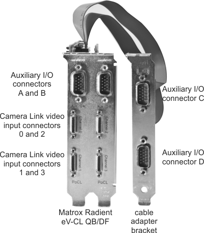
Only the following connectors have auxiliary signals with matching MIL information.
|
Connector Name |
Connector Abbreviation |
Image |
Description |
|
Camera Link video input connectors |
SDR (0,1,2 and 3) |
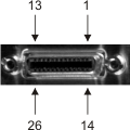
|
The Camera Link video input connectors are 26-pin high-density female mini Camera Link connectors. They are used to receive video input, timing, synchronization signals and transmit/receive communication signals between the video source and the frame grabber. There are two Camera Link video input connectors (SDR 0 and 1) on Matrox Radient eV-CL DB. There are four Camera Link video input connectors (SDR 0, 1, 2 and 3) on Matrox Radient eV-CL QB. |
|
External auxiliary I/O connector |
HD-15 1 (A, B, C and D) |
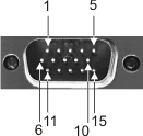
|
The external auxiliary I/O connectors are high-density D-subminiature 15-pin male connectors. They are used to transmit/receive auxiliary signals. External auxiliary I/O connectors A and (if present) B are located on Matrox Radient eV-CL, and external auxiliary I/O connectors C and D are located on the cable adapter bracket. |
1 Previously referred to as DBHD-15, but more accurately known as DE-15.
Signal names and their matching MIL constants
The table below lists the auxiliary signals with their associated MIL information.
|
|
Description | ||
| MIL I/O # | |||
| Pin information | |||
| Direction | |||
| User-bit information | |||
| Trigger information | |||
| Timer information | |||
| Hardware manual signal name | |||
|
Indicates the following. (summarize)Indicates the following. (more details...) |
|||
Shared with: M_DEV1 |
Opto-isolated auxiliary signal (input), shared between acquisition paths 0 and 1 for trigger input or user input. (summarize)Opto-isolated auxiliary signal (input), shared between acquisition paths 0 and 1 for trigger input or user input. (more details...) |
||
| Pin information | Connector: HD-15 (C) Pin: 15+, 9- | ||
| Direction |
Input |
||
| Trigger information | Trigger controller: 0 or 2 on
acq path 1; 2 on acq path 0. M_AUX_IO0; Digitizer device #: M_DEV0, M_DEV1; Trigger controller: 0 or 2 on acq path 1; 2 on acq path 0. |
||
| Hardware manual signal name | OPTO_AUX_IN8 | ||
Shared with: M_DEV1 |
Opto-isolated auxiliary signal (input), shared between acquisition paths 0 and 1 for trigger input or user input. (summarize)Opto-isolated auxiliary signal (input), shared between acquisition paths 0 and 1 for trigger input or user input. (more details...) |
||
| Pin information | Connector: HD-15 (C) Pin: 12+, 11- | ||
| Direction |
Input |
||
| Trigger information | Trigger controller: 1 or 3 on
acq path 1; 3 on acq path 0. M_AUX_IO1; Digitizer device #: M_DEV0, M_DEV1; Trigger controller: 1 or 3 on acq path 1; 3 on acq path 0. |
||
| Hardware manual signal name | OPTO_AUX_IN9 | ||
Shared with: M_DEV1 |
TTL auxiliary signal (input/output), shared between acquisition paths 0 and 1 for trigger input, user input or user output, and dedicated to acquisition path 0 for timer output. (summarize)TTL auxiliary signal (input/output), shared between acquisition paths 0 and 1 for trigger input, user input or user output, and dedicated to acquisition path 0 for timer output. (more details...) |
||
| Pin information | Connector: HD-15 (A) Pin: 3 | ||
| Direction |
Input/Output |
||
| User-bit information |
MIL user-bit #: M_USER_BIT4;
Digitizer device #: M_DEV0,
M_DEV1; |
||
| Trigger information | Trigger controller: 2 on acq
path 0; 2 on acq path 1. M_AUX_IO2; Digitizer device #: M_DEV0, M_DEV1; Trigger controller: 2 on acq path 0; 2 on acq path 1. |
||
| Timer information | Timer: M_TIMER2; Digitizer device #: M_DEV0; | ||
| Hardware manual signal name | TTL_AUX_IO_6 | ||
Shared with: M_DEV1 |
TTL auxiliary signal (input/output), shared between acquisition paths 0 and 1 for trigger input, user input or user output, and dedicated to acquisition path 1 for timer output. (summarize)TTL auxiliary signal (input/output), shared between acquisition paths 0 and 1 for trigger input, user input or user output, and dedicated to acquisition path 1 for timer output. (more details...) |
||
| Pin information | Connector: HD-15 (C) Pin: 3 | ||
| Direction |
Input/Output |
||
| User-bit information |
MIL user-bit #: M_USER_BIT5;
Digitizer device #: M_DEV0,
M_DEV1; |
||
| Trigger information | Trigger controller: 3 on acq
path 0; 3 on acq path 1. M_AUX_IO3; Digitizer device #: M_DEV0, M_DEV1; Trigger controller: 3 on acq path 0; 3 on acq path 1. |
||
| Timer information | Timer: M_TIMER2; Digitizer device #: M_DEV1; | ||
| Hardware manual signal name | TTL_AUX_IO_14 | ||
Shared with: M_DEV1 |
LVDS auxiliary signal (input), shared between acquisition paths 0 and 1 for trigger input or user input, and dedicated to acquisition path 1 for quadrature input bit 0. (summarize)LVDS auxiliary signal (input), shared between acquisition paths 0 and 1 for trigger input or user input, and dedicated to acquisition path 1 for quadrature input bit 0. (more details...) |
||
| Pin information | Connector: HD-15 (C) Pin: 4+, 5- | ||
| Direction |
Input |
||
| Trigger information | Trigger controller: 2 on acq
path 0; 2 or 0 on acq path 1. M_AUX_IO4; Digitizer device #: M_DEV0, M_DEV1; Trigger controller: 2 on acq path 0; 2 or 0 on acq path 1. |
||
| Hardware manual signal name | LVDS_AUX_IN10 | ||
Shared with: M_DEV1 |
LVDS auxiliary signal (input), shared between acquisition paths 0 and 1 for trigger input or user input, and dedicated to acquisition path 1 for timer-clock input or quadrature input bit 1. (summarize)LVDS auxiliary signal (input), shared between acquisition paths 0 and 1 for trigger input or user input, and dedicated to acquisition path 1 for timer-clock input or quadrature input bit 1. (more details...) |
||
| Pin information | Connector: HD-15 (C) Pin: 6+, 8- | ||
| Direction |
Input |
||
| Trigger information | Trigger controller: 1 or 3 on
acq path 1; 3 on acq path 0. M_AUX_IO5; Digitizer device #: M_DEV0, M_DEV1; Trigger controller: 1 or 3 on acq path 1; 3 on acq path 0. |
||
| Hardware manual signal name | LVDS_AUX_IN11 | ||
|
Opto-isolated auxiliary signal (input) for acquisition path 0, which supports: user input or trigger input. (summarize)Opto-isolated auxiliary signal (input) for acquisition path 0, which supports: user input or trigger input. (more details...) |
|||
| Pin information | Connector: HD-15 (A) Pin: 15+, 9- | ||
| Direction |
Input |
||
| Trigger information | Trigger controller: 0 on acq
path 0. M_AUX_IO6; Digitizer device #: M_DEV0; Trigger controller: 0 on acq path 0. |
||
| Hardware manual signal name | OPTO_AUX_IN0 | ||
|
Opto-isolated auxiliary signal (input) for acquisition path 0, which supports: user input or trigger input. (summarize)Opto-isolated auxiliary signal (input) for acquisition path 0, which supports: user input or trigger input. (more details...) |
|||
| Pin information | Connector: HD-15 (A) Pin: 12+, 11- | ||
| Direction |
Input |
||
| Trigger information | Trigger controller: 1 on acq
path 0. M_AUX_IO7; Digitizer device #: M_DEV0; Trigger controller: 1 on acq path 0. |
||
| Hardware manual signal name | OPTO_AUX_IN1 | ||
|
TTL auxiliary signal (input/output) for acquisition path 0, which supports: user input/output, trigger input. (summarize)TTL auxiliary signal (input/output) for acquisition path 0, which supports: user input/output, trigger input. (more details...) |
|||
| Pin information | Connector: HD-15 (A) Pin: 1 | ||
| Direction |
Input/Output |
||
| User-bit information |
MIL user-bit #: M_USER_BIT2;
Digitizer device #: M_DEV0;
|
||
| Trigger information | Trigger controller: 0 on acq
path 0. M_AUX_IO8; Digitizer device #: M_DEV0; Trigger controller: 0 on acq path 0. |
||
| Hardware manual signal name | TTL_AUX_IO_4 | ||
|
TTL auxiliary signal (input/output) for acquisition path 0, which supports: timer output, trigger input, user input, or user output. (summarize)TTL auxiliary signal (input/output) for acquisition path 0, which supports: timer output, trigger input, user input, or user output. (more details...) |
|||
| Pin information | Connector: HD-15 (A) Pin: 2 | ||
| Direction |
Input/Output |
||
| User-bit information |
MIL user-bit #: M_USER_BIT3;
Digitizer device #: M_DEV0;
|
||
| Trigger information | Trigger controller: 1 on acq
path 0. M_AUX_IO9; Digitizer device #: M_DEV0; Trigger controller: 1 on acq path 0. |
||
| Timer information | Timer: M_TIMER1; Digitizer device #: M_DEV0; | ||
| Hardware manual signal name | TTL_AUX_IO_5 | ||
|
LVDS auxiliary signal (input) for acquisition path 0, which supports: trigger input, user input, or quadrature input bit 0. (summarize)LVDS auxiliary signal (input) for acquisition path 0, which supports: trigger input, user input, or quadrature input bit 0. (more details...) |
|||
| Pin information | Connector: HD-15 (A) Pin: 4+, 5- | ||
| Direction |
Input |
||
| Trigger information | Trigger controller: 0 on acq
path 0. M_AUX_IO10; Digitizer device #: M_DEV0; Trigger controller: 0 on acq path 0. |
||
| Hardware manual signal name | LVDS_AUX_IN2 | ||
|
LVDS auxiliary signal (input) for acquisition path 0, which supports: user input, trigger input, timer-clock input, or quadrature input bit 1. (summarize)LVDS auxiliary signal (input) for acquisition path 0, which supports: user input, trigger input, timer-clock input, or quadrature input bit 1. (more details...) |
|||
| Pin information | Connector: HD-15 (A) Pin: 6+, 8- | ||
| Direction |
Input |
||
| Trigger information | Trigger controller: 1 on acq
path 0. M_AUX_IO11; Digitizer device #: M_DEV0; Trigger controller: 1 on acq path 0. |
||
| Hardware manual signal name | LVDS_AUX_IN3 | ||
|
LVDS auxiliary signal (output) for acquisition path 0, which supports: timer output or user output. (summarize)LVDS auxiliary signal (output) for acquisition path 0, which supports: timer output or user output. (more details...) |
|||
| Pin information | Connector: HD-15 (A) Pin: 13+, 14- | ||
| Direction |
Output |
||
| User-bit information |
MIL user-bit #: M_USER_BIT0;
Digitizer device #: M_DEV0;
|
||
| Timer information | Timer: M_TIMER1/M_TIMER2; Digitizer device #: M_DEV0; | ||
| Hardware manual signal name | LVDS_AUX_OUT7 | ||
|
Camera control output 1 for acquisition path 0, which supports: timer output, user output, VSYNC output, HSYNC output, clock output, or rerouting of specific auxiliary input signals. Only the following auxiliary input signals can be rerouted to this output signal: Camera control output 1 for acquisition path 0, which supports: timer output, user output, VSYNC output, HSYNC output, clock output, or rerouting of specific auxiliary input signals. (more details...) |
|||
| Pin information | Connector: HDR/SDR (0) Pin: 5+, 18- | ||
| Direction |
Output |
||
| User-bit information |
MIL user-bit #: M_USER_BIT_CC_IO0/M_USER_BIT_CC_IO1;
Digitizer device #: M_DEV0;
|
||
| Timer information | Timer: M_TIMER1/M_TIMER2; Digitizer device #: M_DEV0; | ||
| Hardware manual signal name | CC1 (0) | ||
|
Camera control output 2 for acquisition path 0, which supports: timer output, user output, VSYNC output, HSYNC output, clock output, or rerouting of specific auxiliary input signals. Only the following auxiliary input signals can be rerouted to this output signal: Camera control output 2 for acquisition path 0, which supports: timer output, user output, VSYNC output, HSYNC output, clock output, or rerouting of specific auxiliary input signals. (more details...) |
|||
| Pin information | Connector: HDR/SDR (0) Pin: 17+, 4- | ||
| Direction |
Output |
||
| User-bit information |
MIL user-bit #: M_USER_BIT_CC_IO0/M_USER_BIT_CC_IO1;
Digitizer device #: M_DEV0;
|
||
| Timer information | Timer: M_TIMER1/M_TIMER2; Digitizer device #: M_DEV0; | ||
| Hardware manual signal name | CC2 (0) | ||
|
Camera control output 3 for acquisition path 0, which supports: timer output, user output, VSYNC output, HSYNC output, clock output, or rerouting of specific auxiliary input signals. Only the following auxiliary input signals can be rerouted to this output signal: Camera control output 3 for acquisition path 0, which supports: timer output, user output, VSYNC output, HSYNC output, clock output, or rerouting of specific auxiliary input signals. (more details...) |
|||
| Pin information | Connector: HDR/SDR (0) Pin: 3+, 16- | ||
| Direction |
Output |
||
| User-bit information |
MIL user-bit #: M_USER_BIT_CC_IO0/M_USER_BIT_CC_IO1;
Digitizer device #: M_DEV0;
|
||
| Timer information | Timer: M_TIMER1/M_TIMER2; Digitizer device #: M_DEV0; | ||
| Hardware manual signal name | CC3 (0) | ||
|
Camera control output 4 for acquisition path 0, which supports: timer output, user output, VSYNC output, HSYNC output, clock output, or rerouting of specific auxiliary input signals. Only the following auxiliary input signals can be rerouted to this output signal: Camera control output 4 for acquisition path 0, which supports: timer output, user output, VSYNC output, HSYNC output, clock output, or rerouting of specific auxiliary input signals. (more details...) |
|||
| Pin information | Connector: HDR/SDR (0) Pin: 15+, 2- | ||
| Direction |
Output |
||
| User-bit information |
MIL user-bit #: M_USER_BIT_CC_IO0/M_USER_BIT_CC_IO1;
Digitizer device #: M_DEV0;
|
||
| Timer information | Timer: M_TIMER1/M_TIMER2; Digitizer device #: M_DEV0; | ||
| Hardware manual signal name | CC4 (0) | ||
|
Indicates the following. (summarize)Indicates the following. (more details...) |
|||
Shared with: M_DEV0 |
Opto-isolated auxiliary signal (input), shared between acquisition paths 0 and 1 for trigger input or user input. (summarize)Opto-isolated auxiliary signal (input), shared between acquisition paths 0 and 1 for trigger input or user input. (more details...) |
||
| Pin information | Connector: HD-15 (C) Pin: 15+, 9- | ||
| Direction |
Input |
||
| Trigger information | Trigger controller: 0 or 2 on
acq path 1; 2 on acq path 0. M_AUX_IO0; Digitizer device #: M_DEV0, M_DEV1; Trigger controller: 0 or 2 on acq path 1; 2 on acq path 0. |
||
| Hardware manual signal name | OPTO_AUX_IN8 | ||
Shared with: M_DEV0 |
Opto-isolated auxiliary signal (input), shared between acquisition paths 0 and 1 for trigger input or user input. (summarize)Opto-isolated auxiliary signal (input), shared between acquisition paths 0 and 1 for trigger input or user input. (more details...) |
||
| Pin information | Connector: HD-15 (C) Pin: 12+, 11- | ||
| Direction |
Input |
||
| Trigger information | Trigger controller: 1 or 3 on
acq path 1; 3 on acq path 0. M_AUX_IO1; Digitizer device #: M_DEV0, M_DEV1; Trigger controller: 1 or 3 on acq path 1; 3 on acq path 0. |
||
| Hardware manual signal name | OPTO_AUX_IN9 | ||
Shared with: M_DEV0 |
TTL auxiliary signal (input/output), shared between acquisition paths 0 and 1 for trigger input, user input or user output, and dedicated to acquisition path 0 for timer output. (summarize)TTL auxiliary signal (input/output), shared between acquisition paths 0 and 1 for trigger input, user input or user output, and dedicated to acquisition path 0 for timer output. (more details...) |
||
| Pin information | Connector: HD-15 (A) Pin: 3 | ||
| Direction |
Input/Output |
||
| User-bit information |
MIL user-bit #: M_USER_BIT4;
Digitizer device #: M_DEV0,
M_DEV1; |
||
| Trigger information | Trigger controller: 2 on acq
path 0; 2 on acq path 1. M_AUX_IO2; Digitizer device #: M_DEV0, M_DEV1; Trigger controller: 2 on acq path 0; 2 on acq path 1. |
||
| Timer information | Timer: M_TIMER2; Digitizer device #: M_DEV0; | ||
| Hardware manual signal name | TTL_AUX_IO_6 | ||
Shared with: M_DEV0 |
TTL auxiliary signal (input/output), shared between acquisition paths 0 and 1 for trigger input, user input or user output, and dedicated to acquisition path 1 for timer output. (summarize)TTL auxiliary signal (input/output), shared between acquisition paths 0 and 1 for trigger input, user input or user output, and dedicated to acquisition path 1 for timer output. (more details...) |
||
| Pin information | Connector: HD-15 (C) Pin: 3 | ||
| Direction |
Input/Output |
||
| User-bit information |
MIL user-bit #: M_USER_BIT5;
Digitizer device #: M_DEV0,
M_DEV1; |
||
| Trigger information | Trigger controller: 3 on acq
path 0; 3 on acq path 1. M_AUX_IO3; Digitizer device #: M_DEV0, M_DEV1; Trigger controller: 3 on acq path 0; 3 on acq path 1. |
||
| Timer information | Timer: M_TIMER2; Digitizer device #: M_DEV1; | ||
| Hardware manual signal name | TTL_AUX_IO_14 | ||
Shared with: M_DEV0 |
LVDS auxiliary signal (input), shared between acquisition paths 0 and 1 for trigger input or user input, and dedicated to acquisition path 1 for quadrature input bit 0. (summarize)LVDS auxiliary signal (input), shared between acquisition paths 0 and 1 for trigger input or user input, and dedicated to acquisition path 1 for quadrature input bit 0. (more details...) |
||
| Pin information | Connector: HD-15 (C) Pin: 4+, 5- | ||
| Direction |
Input |
||
| Trigger information | Trigger controller: 2 on acq
path 0; 2 or 0 on acq path 1. M_AUX_IO4; Digitizer device #: M_DEV0, M_DEV1; Trigger controller: 2 on acq path 0; 2 or 0 on acq path 1. |
||
| Hardware manual signal name | LVDS_AUX_IN10 | ||
Shared with: M_DEV0 |
LVDS auxiliary signal (input), shared between acquisition paths 0 and 1 for trigger input or user input, and dedicated to acquisition path 1 for timer-clock input or quadrature input bit 1. (summarize)LVDS auxiliary signal (input), shared between acquisition paths 0 and 1 for trigger input or user input, and dedicated to acquisition path 1 for timer-clock input or quadrature input bit 1. (more details...) |
||
| Pin information | Connector: HD-15 (C) Pin: 6+, 8- | ||
| Direction |
Input |
||
| Trigger information | Trigger controller: 1 or 3 on
acq path 1; 3 on acq path 0. M_AUX_IO5; Digitizer device #: M_DEV0, M_DEV1; Trigger controller: 1 or 3 on acq path 1; 3 on acq path 0. |
||
| Hardware manual signal name | LVDS_AUX_IN11 | ||
|
TTL auxiliary signal (input/output) for acquisition path 1, which supports: trigger input, user input, or user output. (summarize)TTL auxiliary signal (input/output) for acquisition path 1, which supports: trigger input, user input, or user output. (more details...) |
|||
| Pin information | Connector: HD-15 (C) Pin: 1 | ||
| Direction |
Input/Output |
||
| User-bit information |
MIL user-bit #: M_USER_BIT2;
Digitizer device #: M_DEV1;
|
||
| Trigger information | Trigger controller: 0 on acq
path 1. M_AUX_IO8; Digitizer device #: M_DEV1; Trigger controller: 0 on acq path 1. |
||
| Hardware manual signal name | TTL_AUX_IO_12 | ||
|
TTL auxiliary signal (input/output) for acquisition path 1, which supports: timer output, trigger input, user input, or user output. (summarize)TTL auxiliary signal (input/output) for acquisition path 1, which supports: timer output, trigger input, user input, or user output. (more details...) |
|||
| Pin information | Connector: HD-15 (C) Pin: 2 | ||
| Direction |
Input/Output |
||
| User-bit information |
MIL user-bit #: M_USER_BIT3;
Digitizer device #: M_DEV1;
|
||
| Trigger information | Trigger controller: 1 on acq
path 1. M_AUX_IO9; Digitizer device #: M_DEV1; Trigger controller: 1 on acq path 1. |
||
| Timer information | Timer: M_TIMER1; Digitizer device #: M_DEV1; | ||
| Hardware manual signal name | TTL_AUX_IO_13 | ||
|
LVDS auxiliary signal (output) for acquisition path 1, which supports: timer output or user output. (summarize)LVDS auxiliary signal (output) for acquisition path 1, which supports: timer output or user output. (more details...) |
|||
| Pin information | Connector: HD-15 (C) Pin: 13+, 14- | ||
| Direction |
Output |
||
| User-bit information |
MIL user-bit #: M_USER_BIT0;
Digitizer device #: M_DEV1;
|
||
| Timer information | Timer: M_TIMER1/M_TIMER2; Digitizer device #: M_DEV1; | ||
| Hardware manual signal name | LVDS_AUX_OUT15 | ||
|
Camera control output 1 for acquisition path 1, which supports: timer output, user output, VSYNC output, HSYNC output, clock output, or rerouting of specific auxiliary input signals. Only the following auxiliary input signals can be rerouted to this output signal: Camera control output 1 for acquisition path 1, which supports: timer output, user output, VSYNC output, HSYNC output, clock output, or rerouting of specific auxiliary input signals. (more details...) |
|||
| Pin information | Connector: HDR/SDR (1) Pin: 5+, 18- | ||
| Direction |
Output |
||
| User-bit information |
MIL user-bit #: M_USER_BIT_CC_IO0/M_USER_BIT_CC_IO1;
Digitizer device #: M_DEV1;
|
||
| Timer information | Timer: M_TIMER1/M_TIMER2; Digitizer device #: M_DEV1; | ||
| Hardware manual signal name | CC1 (1) | ||
|
Camera control output 2 for acquisition path 1, which supports: timer output, user output, VSYNC output, HSYNC output, clock output, or rerouting of specific auxiliary input signals. Only the following auxiliary input signals can be rerouted to this output signal: Camera control output 2 for acquisition path 1, which supports: timer output, user output, VSYNC output, HSYNC output, clock output, or rerouting of specific auxiliary input signals. (more details...) |
|||
| Pin information | Connector: HDR/SDR (1) Pin: 17+, 4- | ||
| Direction |
Output |
||
| User-bit information |
MIL user-bit #: M_USER_BIT_CC_IO0/M_USER_BIT_CC_IO1;
Digitizer device #: M_DEV1;
|
||
| Timer information | Timer: M_TIMER1/M_TIMER2; Digitizer device #: M_DEV1; | ||
| Hardware manual signal name | CC2 (1) | ||
|
Camera control output 3 for acquisition path 1, which supports: timer output, user output, VSYNC output, HSYNC output, clock output, or rerouting of specific auxiliary input signals. Only the following auxiliary input signals can be rerouted to this output signal: Camera control output 3 for acquisition path 1, which supports: timer output, user output, VSYNC output, HSYNC output, clock output, or rerouting of specific auxiliary input signals. (more details...) |
|||
| Pin information | Connector: HDR/SDR (1) Pin: 3+, 16- | ||
| Direction |
Output |
||
| User-bit information |
MIL user-bit #: M_USER_BIT_CC_IO0/M_USER_BIT_CC_IO1;
Digitizer device #: M_DEV1;
|
||
| Timer information | Timer: M_TIMER1/M_TIMER2; Digitizer device #: M_DEV1; | ||
| Hardware manual signal name | CC3 (1) | ||
|
Camera control output 4 for acquisition path 1, which supports: timer output, user output, VSYNC output, HSYNC output, clock output, or rerouting of specific auxiliary input signals. Only the following auxiliary input signals can be rerouted to this output signal: Camera control output 4 for acquisition path 1, which supports: timer output, user output, VSYNC output, HSYNC output, clock output, or rerouting of specific auxiliary input signals. (more details...) |
|||
| Pin information | Connector: HDR/SDR (1) Pin: 15+, 2- | ||
| Direction |
Output |
||
| User-bit information |
MIL user-bit #: M_USER_BIT_CC_IO0/M_USER_BIT_CC_IO1;
Digitizer device #: M_DEV1;
|
||
| Timer information | Timer: M_TIMER1/M_TIMER2; Digitizer device #: M_DEV1; | ||
| Hardware manual signal name | CC4 (1) | ||
|
Indicates the following. (summarize)Indicates the following. (more details...) |
|||
Shared with: M_DEV3 2 |
Opto-isolated auxiliary signal (input), shared between acquisition paths 2 and 3 for trigger input or user input. (summarize)Opto-isolated auxiliary signal (input), shared between acquisition paths 2 and 3 for trigger input or user input. (more details...) |
||
| Pin information | Connector: HD-15 (D) Pin: 15+, 9- | ||
| Direction |
Input |
||
| Trigger information | Trigger controller: 0 or 2 on
acq path 3; 2 on acq path 2. M_AUX_IO0; Digitizer device #: M_DEV2 2 , M_DEV3 2 ; Trigger controller: 0 or 2 on acq path 3; 2 on acq path 2. |
||
| Hardware manual signal name | OPTO_AUX_IN24 | ||
Shared with: M_DEV3 2 |
Opto-isolated auxiliary signal (input), shared between acquisition paths 2 and 3 for trigger input or user input. (summarize)Opto-isolated auxiliary signal (input), shared between acquisition paths 2 and 3 for trigger input or user input. (more details...) |
||
| Pin information | Connector: HD-15 (D) Pin: 12+, 11- | ||
| Direction |
Input |
||
| Trigger information | Trigger controller: 1 or 3 on
acq path 3; 3 on acq path 2. M_AUX_IO1; Digitizer device #: M_DEV2 2 , M_DEV3 2 ; Trigger controller: 1 or 3 on acq path 3; 3 on acq path 2. |
||
| Hardware manual signal name | OPTO_AUX_IN25 | ||
Shared with: M_DEV3 2 |
TTL auxiliary signal (input/output), shared between acquisition paths 2 and 3 for trigger input, user input or user output, and dedicated to acquisition path 2 for timer output. (summarize)TTL auxiliary signal (input/output), shared between acquisition paths 2 and 3 for trigger input, user input or user output, and dedicated to acquisition path 2 for timer output. (more details...) |
||
| Pin information | Connector: HD-15 (B) 3 Pin: 3 | ||
| Direction |
Input/Output |
||
| User-bit information | |||
| Trigger information | Trigger controller: 2 on acq
path 2; 2 on acq path 3. M_AUX_IO2; Digitizer device #: M_DEV2 2 , M_DEV3 2 ; Trigger controller: 2 on acq path 2; 2 on acq path 3. |
||
| Timer information | Timer: M_TIMER2; Digitizer device #: M_DEV2 2 ; | ||
| Hardware manual signal name | TTL_AUX_IO_22 | ||
Shared with: M_DEV3 2 |
TTL auxiliary signal (input/output), shared between acquisition paths 2 and 3 for trigger input, user input or user output, and dedicated to acquisition path 3 for timer output. (summarize)TTL auxiliary signal (input/output), shared between acquisition paths 2 and 3 for trigger input, user input or user output, and dedicated to acquisition path 3 for timer output. (more details...) |
||
| Pin information | Connector: HD-15 (D) Pin: 3 | ||
| Direction |
Input/Output |
||
| User-bit information | |||
| Trigger information | Trigger controller: 3 on acq
path 2; 3 on acq path 3. M_AUX_IO3; Digitizer device #: M_DEV2 2 , M_DEV3 2 ; Trigger controller: 3 on acq path 2; 3 on acq path 3. |
||
| Timer information | Timer: M_TIMER2; Digitizer device #: M_DEV3 2 ; | ||
| Hardware manual signal name | TTL_AUX_IO_30 | ||
Shared with: M_DEV3 2 |
LVDS auxiliary signal (input), shared between acquisition paths 2 and 3 for trigger input or user input, and dedicated to acquisition path 3 for quadrature input bit 0. (summarize)LVDS auxiliary signal (input), shared between acquisition paths 2 and 3 for trigger input or user input, and dedicated to acquisition path 3 for quadrature input bit 0. (more details...) |
||
| Pin information | Connector: HD-15 (D) Pin: 4+, 5- | ||
| Direction |
Input |
||
| Trigger information | Trigger controller: 0 or 2 on
acq path 3; 2 on acq path 2. M_AUX_IO4; Digitizer device #: M_DEV2 2 , M_DEV3 2 ; Trigger controller: 0 or 2 on acq path 3; 2 on acq path 2. |
||
| Hardware manual signal name | LVDS_AUX_IN26 | ||
Shared with: M_DEV3 2 |
LVDS auxiliary signal (input), shared between acquisition paths 2 and 3 for trigger input or user input, and dedicated to acquisition path 3 for timer-clock input or quadrature input bit 1. (summarize)LVDS auxiliary signal (input), shared between acquisition paths 2 and 3 for trigger input or user input, and dedicated to acquisition path 3 for timer-clock input or quadrature input bit 1. (more details...) |
||
| Pin information | Connector: HD-15 (D) Pin: 6+, 8- | ||
| Direction |
Input |
||
| Trigger information | Trigger controller: 1 or 3 on
acq path 3; 3 on acq path 2. M_AUX_IO5; Digitizer device #: M_DEV2 2 , M_DEV3 2 ; Trigger controller: 1 or 3 on acq path 3; 3 on acq path 2. |
||
| Hardware manual signal name | LVDS_AUX_IN27 | ||
|
Opto-isolated auxiliary signal (input) for acquisition path 2, which supports: user input or trigger input. (summarize)Opto-isolated auxiliary signal (input) for acquisition path 2, which supports: user input or trigger input. (more details...) |
|||
| Pin information | Connector: HD-15 (B) 3 Pin: 15+, 9- | ||
| Direction |
Input |
||
| Trigger information | Trigger controller: 0 on acq
path 2. M_AUX_IO6; Digitizer device #: M_DEV2 2 ; Trigger controller: 0 on acq path 2. |
||
| Hardware manual signal name | OPTO_AUX_IN16 | ||
|
Opto-isolated auxiliary signal (input) for acquisition path 2, which supports: user input or trigger input. (summarize)Opto-isolated auxiliary signal (input) for acquisition path 2, which supports: user input or trigger input. (more details...) |
|||
| Pin information | Connector: HD-15 (B) 3 Pin: 12+, 11- | ||
| Direction |
Input |
||
| Trigger information | Trigger controller: 1 on acq
path 2. M_AUX_IO7; Digitizer device #: M_DEV2 2 ; Trigger controller: 1 on acq path 2. |
||
| Hardware manual signal name | OPTO_AUX_IN17 | ||
|
TTL auxiliary signal (input/output) for acquisition path 2, which supports: trigger input, user input, or user output. (summarize)TTL auxiliary signal (input/output) for acquisition path 2, which supports: trigger input, user input, or user output. (more details...) |
|||
| Pin information | Connector: HD-15 (B) 3 Pin: 1 | ||
| Direction |
Input/Output |
||
| User-bit information |
MIL user-bit #: M_USER_BIT2;
Digitizer device #: M_DEV2 2 ;
|
||
| Trigger information | Trigger controller: 0 on acq
path 2. M_AUX_IO8; Digitizer device #: M_DEV2 2 ; Trigger controller: 0 on acq path 2. |
||
| Hardware manual signal name | TTL_AUX_IO_20 | ||
|
TTL auxiliary signal (input/output) for acquisition path 2, which supports: timer output, trigger input, user input, or user output. (summarize)TTL auxiliary signal (input/output) for acquisition path 2, which supports: timer output, trigger input, user input, or user output. (more details...) |
|||
| Pin information | Connector: HD-15 (B) 3 Pin: 2 | ||
| Direction |
Input/Output |
||
| User-bit information |
MIL user-bit #: M_USER_BIT3;
Digitizer device #: M_DEV2 2 ;
|
||
| Trigger information | Trigger controller: 1 on acq
path 2. M_AUX_IO9; Digitizer device #: M_DEV2 2 ; Trigger controller: 1 on acq path 2. |
||
| Timer information | Timer: M_TIMER1; Digitizer device #: M_DEV2 2 ; | ||
| Hardware manual signal name | TTL_AUX_IO_21 | ||
|
LVDS auxiliary signal (input) for acquisition path 2, which supports: trigger input, user input, or quadrature input bit 0. (summarize)LVDS auxiliary signal (input) for acquisition path 2, which supports: trigger input, user input, or quadrature input bit 0. (more details...) |
|||
| Pin information | Connector: HD-15 (B) 3 Pin: 4+, 5- | ||
| Direction |
Input |
||
| Trigger information | Trigger controller: 0 on acq
path 2. M_AUX_IO10; Digitizer device #: M_DEV2 2 ; Trigger controller: 0 on acq path 2. |
||
| Hardware manual signal name | LVDS_AUX_IN18 | ||
|
LVDS auxiliary signal (input) for acquisition path 2, which supports: user input, trigger input, timer-clock input, or quadrature input bit 1. (summarize)LVDS auxiliary signal (input) for acquisition path 2, which supports: user input, trigger input, timer-clock input, or quadrature input bit 1. (more details...) |
|||
| Pin information | Connector: HD-15 (B) 3 Pin: 6+, 8- | ||
| Direction |
Input |
||
| Trigger information | Trigger controller: 1 on acq
path 2. M_AUX_IO11; Digitizer device #: M_DEV2 2 ; Trigger controller: 1 on acq path 2. |
||
| Hardware manual signal name | LVDS_AUX_IN19 | ||
|
LVDS auxiliary signal (output) for acquisition path 2, which supports: timer output or user output. (summarize)LVDS auxiliary signal (output) for acquisition path 2, which supports: timer output or user output. (more details...) |
|||
| Pin information | Connector: HD-15 (B) 3 Pin: 13+, 14- | ||
| Direction |
Output |
||
| User-bit information |
MIL user-bit #: M_USER_BIT0;
Digitizer device #: M_DEV2 2 ;
|
||
| Timer information | Timer: M_TIMER1/M_TIMER2; Digitizer device #: M_DEV2 2 ; | ||
| Hardware manual signal name | LVDS_AUX_OUT23 | ||
|
Camera control output 1 for acquisition path 2, which supports: timer output, user output, VSYNC output, HSYNC output, clock output, or rerouting of specific auxiliary input signals. Only the following auxiliary input signals can be rerouted to this output signal: Camera control output 1 for acquisition path 2, which supports: timer output, user output, VSYNC output, HSYNC output, clock output, or rerouting of specific auxiliary input signals. (more details...) |
|||
| Pin information | Connector: HDR/SDR (2) 3 Pin: 5+, 18- | ||
| Direction |
Output |
||
| User-bit information |
MIL user-bit #: M_USER_BIT_CC_IO0/M_USER_BIT_CC_IO1;
Digitizer device #: M_DEV2 2 ;
|
||
| Timer information | Timer: M_TIMER1/M_TIMER2; Digitizer device #: M_DEV2 2 ; | ||
| Hardware manual signal name | CC1 (2) | ||
|
Camera control output 2 for acquisition path 2, which supports: timer output, user output, VSYNC output, HSYNC output, clock output, or rerouting of specific auxiliary input signals. Only the following auxiliary input signals can be rerouted to this output signal: Camera control output 2 for acquisition path 2, which supports: timer output, user output, VSYNC output, HSYNC output, clock output, or rerouting of specific auxiliary input signals. (more details...) |
|||
| Pin information | Connector: HDR/SDR (2) 3 Pin: 17+, 4- | ||
| Direction |
Output |
||
| User-bit information |
MIL user-bit #: M_USER_BIT_CC_IO0/M_USER_BIT_CC_IO1;
Digitizer device #: M_DEV2 2 ;
|
||
| Timer information | Timer: M_TIMER1/M_TIMER2; Digitizer device #: M_DEV2 2 ; | ||
| Hardware manual signal name | CC2 (2) | ||
|
Camera control output 3 for acquisition path 2, which supports: timer output, user output, VSYNC output, HSYNC output, clock output, or rerouting of specific auxiliary input signals. Only the following auxiliary input signals can be rerouted to this output signal: Camera control output 3 for acquisition path 2, which supports: timer output, user output, VSYNC output, HSYNC output, clock output, or rerouting of specific auxiliary input signals. (more details...) |
|||
| Pin information | Connector: HDR/SDR (2) 3 Pin: 3+, 16- | ||
| Direction |
Output |
||
| User-bit information |
MIL user-bit #: M_USER_BIT_CC_IO0/M_USER_BIT_CC_IO1;
Digitizer device #: M_DEV2 2 ;
|
||
| Timer information | Timer: M_TIMER1/M_TIMER2; Digitizer device #: M_DEV2 2 ; | ||
| Hardware manual signal name | CC3 (2) | ||
|
Camera control output 4 for acquisition path 2, which supports: timer output, user output, VSYNC output, HSYNC output, clock output, or rerouting of specific auxiliary input signals. Only the following auxiliary input signals can be rerouted to this output signal: Camera control output 4 for acquisition path 2, which supports: timer output, user output, VSYNC output, HSYNC output, clock output, or rerouting of specific auxiliary input signals. (more details...) |
|||
| Pin information | Connector: HDR/SDR (2) 3 Pin: 15+, 2- | ||
| Direction |
Output |
||
| User-bit information |
MIL user-bit #: M_USER_BIT_CC_IO0/M_USER_BIT_CC_IO1;
Digitizer device #: M_DEV2 2 ;
|
||
| Timer information | Timer: M_TIMER1/M_TIMER2; Digitizer device #: M_DEV2 2 ; | ||
| Hardware manual signal name | CC4 (2) | ||
|
Indicates the following. (summarize)Indicates the following. (more details...) |
|||
Shared with: M_DEV2 2 |
Opto-isolated auxiliary signal (input), shared between acquisition paths 2 and 3 for trigger input or user input. (summarize)Opto-isolated auxiliary signal (input), shared between acquisition paths 2 and 3 for trigger input or user input. (more details...) |
||
| Pin information | Connector: HD-15 (D) Pin: 15+, 9- | ||
| Direction |
Input |
||
| Trigger information | Trigger controller: 0 or 2 on
acq path 3; 2 on acq path 2. M_AUX_IO0; Digitizer device #: M_DEV2 2 , M_DEV3 2 ; Trigger controller: 0 or 2 on acq path 3; 2 on acq path 2. |
||
| Hardware manual signal name | OPTO_AUX_IN24 | ||
Shared with: M_DEV2 2 |
Opto-isolated auxiliary signal (input), shared between acquisition paths 2 and 3 for trigger input or user input. (summarize)Opto-isolated auxiliary signal (input), shared between acquisition paths 2 and 3 for trigger input or user input. (more details...) |
||
| Pin information | Connector: HD-15 (D) Pin: 12+, 11- | ||
| Direction |
Input |
||
| Trigger information | Trigger controller: 1 or 3 on
acq path 3; 3 on acq path 2. M_AUX_IO1; Digitizer device #: M_DEV2 2 , M_DEV3 2 ; Trigger controller: 1 or 3 on acq path 3; 3 on acq path 2. |
||
| Hardware manual signal name | OPTO_AUX_IN25 | ||
Shared with: M_DEV2 2 |
TTL auxiliary signal (input/output), shared between acquisition paths 2 and 3 for trigger input, user input or user output, and dedicated to acquisition path 2 for timer output. (summarize)TTL auxiliary signal (input/output), shared between acquisition paths 2 and 3 for trigger input, user input or user output, and dedicated to acquisition path 2 for timer output. (more details...) |
||
| Pin information | Connector: HD-15 (B) 3 Pin: 3 | ||
| Direction |
Input/Output |
||
| User-bit information | |||
| Trigger information | Trigger controller: 2 on acq
path 2; 2 on acq path 3. M_AUX_IO2; Digitizer device #: M_DEV2 2 , M_DEV3 2 ; Trigger controller: 2 on acq path 2; 2 on acq path 3. |
||
| Timer information | Timer: M_TIMER2; Digitizer device #: M_DEV2 2 ; | ||
| Hardware manual signal name | TTL_AUX_IO_22 | ||
Shared with: M_DEV2 2 |
TTL auxiliary signal (input/output), shared between acquisition paths 2 and 3 for trigger input, user input or user output, and dedicated to acquisition path 3 for timer output. (summarize)TTL auxiliary signal (input/output), shared between acquisition paths 2 and 3 for trigger input, user input or user output, and dedicated to acquisition path 3 for timer output. (more details...) |
||
| Pin information | Connector: HD-15 (D) Pin: 3 | ||
| Direction |
Input/Output |
||
| User-bit information | |||
| Trigger information | Trigger controller: 3 on acq
path 2; 3 on acq path 3. M_AUX_IO3; Digitizer device #: M_DEV2 2 , M_DEV3 2 ; Trigger controller: 3 on acq path 2; 3 on acq path 3. |
||
| Timer information | Timer: M_TIMER2; Digitizer device #: M_DEV3 2 ; | ||
| Hardware manual signal name | TTL_AUX_IO_30 | ||
Shared with: M_DEV2 2 |
LVDS auxiliary signal (input), shared between acquisition paths 2 and 3 for trigger input or user input, and dedicated to acquisition path 3 for quadrature input bit 0. (summarize)LVDS auxiliary signal (input), shared between acquisition paths 2 and 3 for trigger input or user input, and dedicated to acquisition path 3 for quadrature input bit 0. (more details...) |
||
| Pin information | Connector: HD-15 (D) Pin: 4+, 5- | ||
| Direction |
Input |
||
| Trigger information | Trigger controller: 0 or 2 on
acq path 3; 2 on acq path 2. M_AUX_IO4; Digitizer device #: M_DEV2 2 , M_DEV3 2 ; Trigger controller: 0 or 2 on acq path 3; 2 on acq path 2. |
||
| Hardware manual signal name | LVDS_AUX_IN26 | ||
Shared with: M_DEV2 2 |
LVDS auxiliary signal (input), shared between acquisition paths 2 and 3 for trigger input or user input, and dedicated to acquisition path 3 for timer-clock input or quadrature input bit 1. (summarize)LVDS auxiliary signal (input), shared between acquisition paths 2 and 3 for trigger input or user input, and dedicated to acquisition path 3 for timer-clock input or quadrature input bit 1. (more details...) |
||
| Pin information | Connector: HD-15 (D) Pin: 6+, 8- | ||
| Direction |
Input |
||
| Trigger information | Trigger controller: 1 or 3 on
acq path 3; 3 on acq path 2. M_AUX_IO5; Digitizer device #: M_DEV2 2 , M_DEV3 2 ; Trigger controller: 1 or 3 on acq path 3; 3 on acq path 2. |
||
| Hardware manual signal name | LVDS_AUX_IN27 | ||
|
TTL auxiliary signal (input/output) for acquisition path 3, which supports: trigger input, user input, or user output. (summarize)TTL auxiliary signal (input/output) for acquisition path 3, which supports: trigger input, user input, or user output. (more details...) |
|||
| Pin information | Connector: HD-15 (D) Pin: 1 | ||
| Direction |
Input/Output |
||
| User-bit information |
MIL user-bit #: M_USER_BIT2;
Digitizer device #: M_DEV3 2 ;
|
||
| Trigger information | Trigger controller: 0 on acq
path 3. M_AUX_IO8; Digitizer device #: M_DEV3 2 ; Trigger controller: 0 on acq path 3. |
||
| Hardware manual signal name | TTL_AUX_IO_28 | ||
|
TTL auxiliary signal (input/output) for acquisition path 3, which supports: timer output, trigger input, user input, or user output. (summarize)TTL auxiliary signal (input/output) for acquisition path 3, which supports: timer output, trigger input, user input, or user output. (more details...) |
|||
| Pin information | Connector: HD-15 (D) Pin: 2 | ||
| Direction |
Input/Output |
||
| User-bit information |
MIL user-bit #: M_USER_BIT3;
Digitizer device #: M_DEV3 2 ;
|
||
| Trigger information | Trigger controller: 1 on acq
path 3. M_AUX_IO9; Digitizer device #: M_DEV3 2 ; Trigger controller: 1 on acq path 3. |
||
| Timer information | Timer: M_TIMER1; Digitizer device #: M_DEV3 2 ; | ||
| Hardware manual signal name | TTL_AUX_IO_29 | ||
|
LVDS auxiliary signal (output) for acquisition path 3, which supports: timer output or user output. (summarize)LVDS auxiliary signal (output) for acquisition path 3, which supports: timer output or user output. (more details...) |
|||
| Pin information | Connector: HD-15 (D) Pin: 13+, 14- | ||
| Direction |
Output |
||
| User-bit information |
MIL user-bit #: M_USER_BIT0;
Digitizer device #: M_DEV3 2 ;
|
||
| Timer information | Timer: M_TIMER1/M_TIMER2; Digitizer device #: M_DEV3 2 ; | ||
| Hardware manual signal name | LVDS_AUX_OUT31 | ||
|
Camera control output 1 for acquisition path 3, which supports: timer output, user output, VSYNC output, HSYNC output, clock output, or rerouting of specific auxiliary input signals. Only the following auxiliary input signals can be rerouted to this output signal: Camera control output 1 for acquisition path 3, which supports: timer output, user output, VSYNC output, HSYNC output, clock output, or rerouting of specific auxiliary input signals. (more details...) |
|||
| Pin information | Connector: HDR/SDR (3) 3 Pin: 5+, 18- | ||
| Direction |
Output |
||
| User-bit information |
MIL user-bit #: M_USER_BIT_CC_IO0/M_USER_BIT_CC_IO1;
Digitizer device #: M_DEV3 2 ;
|
||
| Timer information | Timer: M_TIMER1/M_TIMER2; Digitizer device #: M_DEV3 2 ; | ||
| Hardware manual signal name | CC1 (3) | ||
|
Camera control output 2 for acquisition path 3, which supports: timer output, user output, VSYNC output, HSYNC output, clock output, or rerouting of specific auxiliary input signals. Only the following auxiliary input signals can be rerouted to this output signal: Camera control output 2 for acquisition path 3, which supports: timer output, user output, VSYNC output, HSYNC output, clock output, or rerouting of specific auxiliary input signals. (more details...) |
|||
| Pin information | Connector: HDR/SDR (3) 3 Pin: 17+, 4- | ||
| Direction |
Output |
||
| User-bit information |
MIL user-bit #: M_USER_BIT_CC_IO0/M_USER_BIT_CC_IO1;
Digitizer device #: M_DEV3 2 ;
|
||
| Timer information | Timer: M_TIMER1/M_TIMER2; Digitizer device #: M_DEV3 2 ; | ||
| Hardware manual signal name | CC2 (3) | ||
|
Camera control output 3 for acquisition path 3, which supports: timer output, user output, VSYNC output, HSYNC output, clock output, or rerouting of specific auxiliary input signals. Only the following auxiliary input signals can be rerouted to this output signal: Camera control output 3 for acquisition path 3, which supports: timer output, user output, VSYNC output, HSYNC output, clock output, or rerouting of specific auxiliary input signals. (more details...) |
|||
| Pin information | Connector: HDR/SDR (3) 3 Pin: 3+, 16- | ||
| Direction |
Output |
||
| User-bit information |
MIL user-bit #: M_USER_BIT_CC_IO0/M_USER_BIT_CC_IO1;
Digitizer device #: M_DEV3 2 ;
|
||
| Timer information | Timer: M_TIMER1/M_TIMER2; Digitizer device #: M_DEV3 2 ; | ||
| Hardware manual signal name | CC3 (3) | ||
|
Camera control output 4 for acquisition path 3, which supports: timer output, user output, VSYNC output, HSYNC output, clock output, or rerouting of specific auxiliary input signals. Only the following auxiliary input signals can be rerouted to this output signal: Camera control output 4 for acquisition path 3, which supports: timer output, user output, VSYNC output, HSYNC output, clock output, or rerouting of specific auxiliary input signals. (more details...) |
|||
| Pin information | Connector: HDR/SDR (3) 3 Pin: 15+, 2- | ||
| Direction |
Output |
||
| User-bit information |
MIL user-bit #: M_USER_BIT_CC_IO0/M_USER_BIT_CC_IO1;
Digitizer device #: M_DEV3 2 ;
|
||
| Timer information | Timer: M_TIMER1/M_TIMER2; Digitizer device #: M_DEV3 2 ; | ||
| Hardware manual signal name | CC4 (3) | ||
|
|
Description | ||
| MIL I/O # | |||
| Pin information | |||
| Direction | |||
| User-bit information | |||
| Trigger information | |||
| Timer information | |||
| Hardware manual signal name | |||
|
Indicates the following. (summarize)Indicates the following. (more details...) |
|||
Shared with: M_DEV1 |
Opto-isolated auxiliary signal (input), shared between acquisition paths 0 and 1 for trigger input or user input. (summarize)Opto-isolated auxiliary signal (input), shared between acquisition paths 0 and 1 for trigger input or user input. (more details...) |
||
| Pin information | Connector: HD-15 (C) Pin: 15+, 9- | ||
| Direction |
Input |
||
| Trigger information | Trigger controller: 0 or 2 on
acq path 1; 2 on acq path 0. M_AUX_IO0; Digitizer device #: M_DEV0, M_DEV1; Trigger controller: 0 or 2 on acq path 1; 2 on acq path 0. |
||
| Hardware manual signal name | OPTO_AUX_IN8 | ||
Shared with: M_DEV1 |
Opto-isolated auxiliary signal (input), shared between acquisition paths 0 and 1 for trigger input or user input. (summarize)Opto-isolated auxiliary signal (input), shared between acquisition paths 0 and 1 for trigger input or user input. (more details...) |
||
| Pin information | Connector: HD-15 (C) Pin: 12+, 11- | ||
| Direction |
Input |
||
| Trigger information | Trigger controller: 1 or 3 on
acq path 1; 3 on acq path 0. M_AUX_IO1; Digitizer device #: M_DEV0, M_DEV1; Trigger controller: 1 or 3 on acq path 1; 3 on acq path 0. |
||
| Hardware manual signal name | OPTO_AUX_IN9 | ||
Shared with: M_DEV1 |
TTL auxiliary signal (input/output), shared between acquisition paths 0 and 1 for trigger input, user input or user output, and dedicated to acquisition path 0 for timer output. (summarize)TTL auxiliary signal (input/output), shared between acquisition paths 0 and 1 for trigger input, user input or user output, and dedicated to acquisition path 0 for timer output. (more details...) |
||
| Pin information | Connector: HD-15 (A) Pin: 3 | ||
| Direction |
Input/Output |
||
| User-bit information |
MIL user-bit #: M_USER_BIT4;
Digitizer device #: M_DEV0,
M_DEV1; |
||
| Trigger information | Trigger controller: 2 on acq
path 0; 2 on acq path 1. M_AUX_IO2; Digitizer device #: M_DEV0, M_DEV1; Trigger controller: 2 on acq path 0; 2 on acq path 1. |
||
| Timer information | Timer: M_TIMER2; Digitizer device #: M_DEV0; | ||
| Hardware manual signal name | TTL_AUX_IO_6 | ||
Shared with: M_DEV1 |
TTL auxiliary signal (input/output), shared between acquisition paths 0 and 1 for trigger input, user input or user output, and dedicated to acquisition path 1 for timer output. (summarize)TTL auxiliary signal (input/output), shared between acquisition paths 0 and 1 for trigger input, user input or user output, and dedicated to acquisition path 1 for timer output. (more details...) |
||
| Pin information | Connector: HD-15 (C) Pin: 3 | ||
| Direction |
Input/Output |
||
| User-bit information |
MIL user-bit #: M_USER_BIT5;
Digitizer device #: M_DEV0,
M_DEV1; |
||
| Trigger information | Trigger controller: 3 on acq
path 0; 3 on acq path 1. M_AUX_IO3; Digitizer device #: M_DEV0, M_DEV1; Trigger controller: 3 on acq path 0; 3 on acq path 1. |
||
| Timer information | Timer: M_TIMER2; Digitizer device #: M_DEV1; | ||
| Hardware manual signal name | TTL_AUX_IO_14 | ||
Shared with: M_DEV1 |
LVDS auxiliary signal (input), shared between acquisition paths 0 and 1 for trigger input or user input, and dedicated to acquisition path 1 for quadrature input bit 0. (summarize)LVDS auxiliary signal (input), shared between acquisition paths 0 and 1 for trigger input or user input, and dedicated to acquisition path 1 for quadrature input bit 0. (more details...) |
||
| Pin information | Connector: HD-15 (C) Pin: 4+, 5- | ||
| Direction |
Input |
||
| Trigger information | Trigger controller: 2 on acq
path 0; 2 or 0 on acq path 1. M_AUX_IO4; Digitizer device #: M_DEV0, M_DEV1; Trigger controller: 2 on acq path 0; 2 or 0 on acq path 1. |
||
| Hardware manual signal name | LVDS_AUX_IN10 | ||
Shared with: M_DEV1 |
LVDS auxiliary signal (input), shared between acquisition paths 0 and 1 for trigger input or user input, and dedicated to acquisition path 1 for timer-clock input or quadrature input bit 1. (summarize)LVDS auxiliary signal (input), shared between acquisition paths 0 and 1 for trigger input or user input, and dedicated to acquisition path 1 for timer-clock input or quadrature input bit 1. (more details...) |
||
| Pin information | Connector: HD-15 (C) Pin: 6+, 8- | ||
| Direction |
Input |
||
| Trigger information | Trigger controller: 1 or 3 on
acq path 1; 3 on acq path 0. M_AUX_IO5; Digitizer device #: M_DEV0, M_DEV1; Trigger controller: 1 or 3 on acq path 1; 3 on acq path 0. |
||
| Hardware manual signal name | LVDS_AUX_IN11 | ||
|
Opto-isolated auxiliary signal (input) for acquisition path 0, which supports: user input or trigger input. (summarize)Opto-isolated auxiliary signal (input) for acquisition path 0, which supports: user input or trigger input. (more details...) |
|||
| Pin information | Connector: HD-15 (A) Pin: 15+, 9- | ||
| Direction |
Input |
||
| Trigger information | Trigger controller: 0 on acq
path 0. M_AUX_IO6; Digitizer device #: M_DEV0; Trigger controller: 0 on acq path 0. |
||
| Hardware manual signal name | OPTO_AUX_IN0 | ||
|
Opto-isolated auxiliary signal (input) for acquisition path 0, which supports: user input or trigger input. (summarize)Opto-isolated auxiliary signal (input) for acquisition path 0, which supports: user input or trigger input. (more details...) |
|||
| Pin information | Connector: HD-15 (A) Pin: 12+, 11- | ||
| Direction |
Input |
||
| Trigger information | Trigger controller: 1 on acq
path 0. M_AUX_IO7; Digitizer device #: M_DEV0; Trigger controller: 1 on acq path 0. |
||
| Hardware manual signal name | OPTO_AUX_IN1 | ||
|
TTL auxiliary signal (input/output) for acquisition path 0, which supports: user input/output, trigger input. (summarize)TTL auxiliary signal (input/output) for acquisition path 0, which supports: user input/output, trigger input. (more details...) |
|||
| Pin information | Connector: HD-15 (A) Pin: 1 | ||
| Direction |
Input/Output |
||
| User-bit information |
MIL user-bit #: M_USER_BIT2;
Digitizer device #: M_DEV0;
|
||
| Trigger information | Trigger controller: 0 on acq
path 0. M_AUX_IO8; Digitizer device #: M_DEV0; Trigger controller: 0 on acq path 0. |
||
| Hardware manual signal name | TTL_AUX_IO_4 | ||
|
TTL auxiliary signal (input/output) for acquisition path 0, which supports: timer output, trigger input, user input, or user output. (summarize)TTL auxiliary signal (input/output) for acquisition path 0, which supports: timer output, trigger input, user input, or user output. (more details...) |
|||
| Pin information | Connector: HD-15 (A) Pin: 2 | ||
| Direction |
Input/Output |
||
| User-bit information |
MIL user-bit #: M_USER_BIT3;
Digitizer device #: M_DEV0;
|
||
| Trigger information | Trigger controller: 1 on acq
path 0. M_AUX_IO9; Digitizer device #: M_DEV0; Trigger controller: 1 on acq path 0. |
||
| Timer information | Timer: M_TIMER1; Digitizer device #: M_DEV0; | ||
| Hardware manual signal name | TTL_AUX_IO_5 | ||
|
LVDS auxiliary signal (input) for acquisition path 0, which supports: trigger input, user input, or quadrature input bit 0. (summarize)LVDS auxiliary signal (input) for acquisition path 0, which supports: trigger input, user input, or quadrature input bit 0. (more details...) |
|||
| Pin information | Connector: HD-15 (A) Pin: 4+, 5- | ||
| Direction |
Input |
||
| Trigger information | Trigger controller: 0 on acq
path 0. M_AUX_IO10; Digitizer device #: M_DEV0; Trigger controller: 0 on acq path 0. |
||
| Hardware manual signal name | LVDS_AUX_IN2 | ||
|
LVDS auxiliary signal (input) for acquisition path 0, which supports: user input, trigger input, timer-clock input, or quadrature input bit 1. (summarize)LVDS auxiliary signal (input) for acquisition path 0, which supports: user input, trigger input, timer-clock input, or quadrature input bit 1. (more details...) |
|||
| Pin information | Connector: HD-15 (A) Pin: 6+, 8- | ||
| Direction |
Input |
||
| Trigger information | Trigger controller: 1 on acq
path 0. M_AUX_IO11; Digitizer device #: M_DEV0; Trigger controller: 1 on acq path 0. |
||
| Hardware manual signal name | LVDS_AUX_IN3 | ||
|
Indicates the following. (summarize)Indicates the following. (more details...) |
|||
Shared with: M_DEV0 |
Opto-isolated auxiliary signal (input), shared between acquisition paths 0 and 1 for trigger input or user input. (summarize)Opto-isolated auxiliary signal (input), shared between acquisition paths 0 and 1 for trigger input or user input. (more details...) |
||
| Pin information | Connector: HD-15 (C) Pin: 15+, 9- | ||
| Direction |
Input |
||
| Trigger information | Trigger controller: 0 or 2 on
acq path 1; 2 on acq path 0. M_AUX_IO0; Digitizer device #: M_DEV0, M_DEV1; Trigger controller: 0 or 2 on acq path 1; 2 on acq path 0. |
||
| Hardware manual signal name | OPTO_AUX_IN8 | ||
Shared with: M_DEV0 |
Opto-isolated auxiliary signal (input), shared between acquisition paths 0 and 1 for trigger input or user input. (summarize)Opto-isolated auxiliary signal (input), shared between acquisition paths 0 and 1 for trigger input or user input. (more details...) |
||
| Pin information | Connector: HD-15 (C) Pin: 12+, 11- | ||
| Direction |
Input |
||
| Trigger information | Trigger controller: 1 or 3 on
acq path 1; 3 on acq path 0. M_AUX_IO1; Digitizer device #: M_DEV0, M_DEV1; Trigger controller: 1 or 3 on acq path 1; 3 on acq path 0. |
||
| Hardware manual signal name | OPTO_AUX_IN9 | ||
Shared with: M_DEV0 |
TTL auxiliary signal (input/output), shared between acquisition paths 0 and 1 for trigger input, user input or user output, and dedicated to acquisition path 0 for timer output. (summarize)TTL auxiliary signal (input/output), shared between acquisition paths 0 and 1 for trigger input, user input or user output, and dedicated to acquisition path 0 for timer output. (more details...) |
||
| Pin information | Connector: HD-15 (A) Pin: 3 | ||
| Direction |
Input/Output |
||
| User-bit information |
MIL user-bit #: M_USER_BIT4;
Digitizer device #: M_DEV0,
M_DEV1; |
||
| Trigger information | Trigger controller: 2 on acq
path 0; 2 on acq path 1. M_AUX_IO2; Digitizer device #: M_DEV0, M_DEV1; Trigger controller: 2 on acq path 0; 2 on acq path 1. |
||
| Timer information | Timer: M_TIMER2; Digitizer device #: M_DEV0; | ||
| Hardware manual signal name | TTL_AUX_IO_6 | ||
Shared with: M_DEV0 |
TTL auxiliary signal (input/output), shared between acquisition paths 0 and 1 for trigger input, user input or user output, and dedicated to acquisition path 1 for timer output. (summarize)TTL auxiliary signal (input/output), shared between acquisition paths 0 and 1 for trigger input, user input or user output, and dedicated to acquisition path 1 for timer output. (more details...) |
||
| Pin information | Connector: HD-15 (C) Pin: 3 | ||
| Direction |
Input/Output |
||
| User-bit information |
MIL user-bit #: M_USER_BIT5;
Digitizer device #: M_DEV0,
M_DEV1; |
||
| Trigger information | Trigger controller: 3 on acq
path 0; 3 on acq path 1. M_AUX_IO3; Digitizer device #: M_DEV0, M_DEV1; Trigger controller: 3 on acq path 0; 3 on acq path 1. |
||
| Timer information | Timer: M_TIMER2; Digitizer device #: M_DEV1; | ||
| Hardware manual signal name | TTL_AUX_IO_14 | ||
Shared with: M_DEV0 |
LVDS auxiliary signal (input), shared between acquisition paths 0 and 1 for trigger input or user input, and dedicated to acquisition path 1 for quadrature input bit 0. (summarize)LVDS auxiliary signal (input), shared between acquisition paths 0 and 1 for trigger input or user input, and dedicated to acquisition path 1 for quadrature input bit 0. (more details...) |
||
| Pin information | Connector: HD-15 (C) Pin: 4+, 5- | ||
| Direction |
Input |
||
| Trigger information | Trigger controller: 2 on acq
path 0; 2 or 0 on acq path 1. M_AUX_IO4; Digitizer device #: M_DEV0, M_DEV1; Trigger controller: 2 on acq path 0; 2 or 0 on acq path 1. |
||
| Hardware manual signal name | LVDS_AUX_IN10 | ||
Shared with: M_DEV0 |
LVDS auxiliary signal (input), shared between acquisition paths 0 and 1 for trigger input or user input, and dedicated to acquisition path 1 for timer-clock input or quadrature input bit 1. (summarize)LVDS auxiliary signal (input), shared between acquisition paths 0 and 1 for trigger input or user input, and dedicated to acquisition path 1 for timer-clock input or quadrature input bit 1. (more details...) |
||
| Pin information | Connector: HD-15 (C) Pin: 6+, 8- | ||
| Direction |
Input |
||
| Trigger information | Trigger controller: 1 or 3 on
acq path 1; 3 on acq path 0. M_AUX_IO5; Digitizer device #: M_DEV0, M_DEV1; Trigger controller: 1 or 3 on acq path 1; 3 on acq path 0. |
||
| Hardware manual signal name | LVDS_AUX_IN11 | ||
|
TTL auxiliary signal (input/output) for acquisition path 1, which supports: trigger input, user input, or user output. (summarize)TTL auxiliary signal (input/output) for acquisition path 1, which supports: trigger input, user input, or user output. (more details...) |
|||
| Pin information | Connector: HD-15 (C) Pin: 1 | ||
| Direction |
Input/Output |
||
| User-bit information |
MIL user-bit #: M_USER_BIT2;
Digitizer device #: M_DEV1;
|
||
| Trigger information | Trigger controller: 0 on acq
path 1. M_AUX_IO8; Digitizer device #: M_DEV1; Trigger controller: 0 on acq path 1. |
||
| Hardware manual signal name | TTL_AUX_IO_12 | ||
|
TTL auxiliary signal (input/output) for acquisition path 1, which supports: timer output, trigger input, user input, or user output. (summarize)TTL auxiliary signal (input/output) for acquisition path 1, which supports: timer output, trigger input, user input, or user output. (more details...) |
|||
| Pin information | Connector: HD-15 (C) Pin: 2 | ||
| Direction |
Input/Output |
||
| User-bit information |
MIL user-bit #: M_USER_BIT3;
Digitizer device #: M_DEV1;
|
||
| Trigger information | Trigger controller: 1 on acq
path 1. M_AUX_IO9; Digitizer device #: M_DEV1; Trigger controller: 1 on acq path 1. |
||
| Timer information | Timer: M_TIMER1; Digitizer device #: M_DEV1; | ||
| Hardware manual signal name | TTL_AUX_IO_13 | ||
|
Indicates the following. (summarize)Indicates the following. (more details...) |
|||
Shared with: M_DEV3 2 |
Opto-isolated auxiliary signal (input), shared between acquisition paths 2 and 3 for trigger input or user input. (summarize)Opto-isolated auxiliary signal (input), shared between acquisition paths 2 and 3 for trigger input or user input. (more details...) |
||
| Pin information | Connector: HD-15 (D) Pin: 15+, 9- | ||
| Direction |
Input |
||
| Trigger information | Trigger controller: 0 or 2 on
acq path 3; 2 on acq path 2. M_AUX_IO0; Digitizer device #: M_DEV2 2 , M_DEV3 2 ; Trigger controller: 0 or 2 on acq path 3; 2 on acq path 2. |
||
| Hardware manual signal name | OPTO_AUX_IN24 | ||
Shared with: M_DEV3 2 |
Opto-isolated auxiliary signal (input), shared between acquisition paths 2 and 3 for trigger input or user input. (summarize)Opto-isolated auxiliary signal (input), shared between acquisition paths 2 and 3 for trigger input or user input. (more details...) |
||
| Pin information | Connector: HD-15 (D) Pin: 12+, 11- | ||
| Direction |
Input |
||
| Trigger information | Trigger controller: 1 or 3 on
acq path 3; 3 on acq path 2. M_AUX_IO1; Digitizer device #: M_DEV2 2 , M_DEV3 2 ; Trigger controller: 1 or 3 on acq path 3; 3 on acq path 2. |
||
| Hardware manual signal name | OPTO_AUX_IN25 | ||
Shared with: M_DEV3 2 |
TTL auxiliary signal (input/output), shared between acquisition paths 2 and 3 for trigger input, user input or user output, and dedicated to acquisition path 2 for timer output. (summarize)TTL auxiliary signal (input/output), shared between acquisition paths 2 and 3 for trigger input, user input or user output, and dedicated to acquisition path 2 for timer output. (more details...) |
||
| Pin information | Connector: HD-15 (B) 3 Pin: 3 | ||
| Direction |
Input/Output |
||
| User-bit information | |||
| Trigger information | Trigger controller: 2 on acq
path 2; 2 on acq path 3. M_AUX_IO2; Digitizer device #: M_DEV2 2 , M_DEV3 2 ; Trigger controller: 2 on acq path 2; 2 on acq path 3. |
||
| Timer information | Timer: M_TIMER2; Digitizer device #: M_DEV2 2 ; | ||
| Hardware manual signal name | TTL_AUX_IO_22 | ||
Shared with: M_DEV3 2 |
TTL auxiliary signal (input/output), shared between acquisition paths 2 and 3 for trigger input, user input or user output, and dedicated to acquisition path 3 for timer output. (summarize)TTL auxiliary signal (input/output), shared between acquisition paths 2 and 3 for trigger input, user input or user output, and dedicated to acquisition path 3 for timer output. (more details...) |
||
| Pin information | Connector: HD-15 (D) Pin: 3 | ||
| Direction |
Input/Output |
||
| User-bit information | |||
| Trigger information | Trigger controller: 3 on acq
path 2; 3 on acq path 3. M_AUX_IO3; Digitizer device #: M_DEV2 2 , M_DEV3 2 ; Trigger controller: 3 on acq path 2; 3 on acq path 3. |
||
| Timer information | Timer: M_TIMER2; Digitizer device #: M_DEV3 2 ; | ||
| Hardware manual signal name | TTL_AUX_IO_30 | ||
Shared with: M_DEV3 2 |
LVDS auxiliary signal (input), shared between acquisition paths 2 and 3 for trigger input or user input, and dedicated to acquisition path 3 for quadrature input bit 0. (summarize)LVDS auxiliary signal (input), shared between acquisition paths 2 and 3 for trigger input or user input, and dedicated to acquisition path 3 for quadrature input bit 0. (more details...) |
||
| Pin information | Connector: HD-15 (D) Pin: 4+, 5- | ||
| Direction |
Input |
||
| Trigger information | Trigger controller: 0 or 2 on
acq path 3; 2 on acq path 2. M_AUX_IO4; Digitizer device #: M_DEV2 2 , M_DEV3 2 ; Trigger controller: 0 or 2 on acq path 3; 2 on acq path 2. |
||
| Hardware manual signal name | LVDS_AUX_IN26 | ||
Shared with: M_DEV3 2 |
LVDS auxiliary signal (input), shared between acquisition paths 2 and 3 for trigger input or user input, and dedicated to acquisition path 3 for timer-clock input or quadrature input bit 1. (summarize)LVDS auxiliary signal (input), shared between acquisition paths 2 and 3 for trigger input or user input, and dedicated to acquisition path 3 for timer-clock input or quadrature input bit 1. (more details...) |
||
| Pin information | Connector: HD-15 (D) Pin: 6+, 8- | ||
| Direction |
Input |
||
| Trigger information | Trigger controller: 1 or 3 on
acq path 3; 3 on acq path 2. M_AUX_IO5; Digitizer device #: M_DEV2 2 , M_DEV3 2 ; Trigger controller: 1 or 3 on acq path 3; 3 on acq path 2. |
||
| Hardware manual signal name | LVDS_AUX_IN27 | ||
|
Opto-isolated auxiliary signal (input) for acquisition path 2, which supports: user input or trigger input. (summarize)Opto-isolated auxiliary signal (input) for acquisition path 2, which supports: user input or trigger input. (more details...) |
|||
| Pin information | Connector: HD-15 (B) 3 Pin: 15+, 9- | ||
| Direction |
Input |
||
| Trigger information | Trigger controller: 0 on acq
path 2. M_AUX_IO6; Digitizer device #: M_DEV2 2 ; Trigger controller: 0 on acq path 2. |
||
| Hardware manual signal name | OPTO_AUX_IN16 | ||
|
Opto-isolated auxiliary signal (input) for acquisition path 2, which supports: user input or trigger input. (summarize)Opto-isolated auxiliary signal (input) for acquisition path 2, which supports: user input or trigger input. (more details...) |
|||
| Pin information | Connector: HD-15 (B) 3 Pin: 12+, 11- | ||
| Direction |
Input |
||
| Trigger information | Trigger controller: 1 on acq
path 2. M_AUX_IO7; Digitizer device #: M_DEV2 2 ; Trigger controller: 1 on acq path 2. |
||
| Hardware manual signal name | OPTO_AUX_IN17 | ||
|
TTL auxiliary signal (input/output) for acquisition path 2, which supports: trigger input, user input, or user output. (summarize)TTL auxiliary signal (input/output) for acquisition path 2, which supports: trigger input, user input, or user output. (more details...) |
|||
| Pin information | Connector: HD-15 (B) 3 Pin: 1 | ||
| Direction |
Input/Output |
||
| User-bit information |
MIL user-bit #: M_USER_BIT2;
Digitizer device #: M_DEV2 2 ;
|
||
| Trigger information | Trigger controller: 0 on acq
path 2. M_AUX_IO8; Digitizer device #: M_DEV2 2 ; Trigger controller: 0 on acq path 2. |
||
| Hardware manual signal name | TTL_AUX_IO_20 | ||
|
TTL auxiliary signal (input/output) for acquisition path 2, which supports: timer output, trigger input, user input, or user output. (summarize)TTL auxiliary signal (input/output) for acquisition path 2, which supports: timer output, trigger input, user input, or user output. (more details...) |
|||
| Pin information | Connector: HD-15 (B) 3 Pin: 2 | ||
| Direction |
Input/Output |
||
| User-bit information |
MIL user-bit #: M_USER_BIT3;
Digitizer device #: M_DEV2 2 ;
|
||
| Trigger information | Trigger controller: 1 on acq
path 2. M_AUX_IO9; Digitizer device #: M_DEV2 2 ; Trigger controller: 1 on acq path 2. |
||
| Timer information | Timer: M_TIMER1; Digitizer device #: M_DEV2 2 ; | ||
| Hardware manual signal name | TTL_AUX_IO_21 | ||
|
LVDS auxiliary signal (input) for acquisition path 2, which supports: trigger input, user input, or quadrature input bit 0. (summarize)LVDS auxiliary signal (input) for acquisition path 2, which supports: trigger input, user input, or quadrature input bit 0. (more details...) |
|||
| Pin information | Connector: HD-15 (B) 3 Pin: 4+, 5- | ||
| Direction |
Input |
||
| Trigger information | Trigger controller: 0 on acq
path 2. M_AUX_IO10; Digitizer device #: M_DEV2 2 ; Trigger controller: 0 on acq path 2. |
||
| Hardware manual signal name | LVDS_AUX_IN18 | ||
|
LVDS auxiliary signal (input) for acquisition path 2, which supports: user input, trigger input, timer-clock input, or quadrature input bit 1. (summarize)LVDS auxiliary signal (input) for acquisition path 2, which supports: user input, trigger input, timer-clock input, or quadrature input bit 1. (more details...) |
|||
| Pin information | Connector: HD-15 (B) 3 Pin: 6+, 8- | ||
| Direction |
Input |
||
| Trigger information | Trigger controller: 1 on acq
path 2. M_AUX_IO11; Digitizer device #: M_DEV2 2 ; Trigger controller: 1 on acq path 2. |
||
| Hardware manual signal name | LVDS_AUX_IN19 | ||
|
Indicates the following. (summarize)Indicates the following. (more details...) |
|||
Shared with: M_DEV2 2 |
Opto-isolated auxiliary signal (input), shared between acquisition paths 2 and 3 for trigger input or user input. (summarize)Opto-isolated auxiliary signal (input), shared between acquisition paths 2 and 3 for trigger input or user input. (more details...) |
||
| Pin information | Connector: HD-15 (D) Pin: 15+, 9- | ||
| Direction |
Input |
||
| Trigger information | Trigger controller: 0 or 2 on
acq path 3; 2 on acq path 2. M_AUX_IO0; Digitizer device #: M_DEV2 2 , M_DEV3 2 ; Trigger controller: 0 or 2 on acq path 3; 2 on acq path 2. |
||
| Hardware manual signal name | OPTO_AUX_IN24 | ||
Shared with: M_DEV2 2 |
Opto-isolated auxiliary signal (input), shared between acquisition paths 2 and 3 for trigger input or user input. (summarize)Opto-isolated auxiliary signal (input), shared between acquisition paths 2 and 3 for trigger input or user input. (more details...) |
||
| Pin information | Connector: HD-15 (D) Pin: 12+, 11- | ||
| Direction |
Input |
||
| Trigger information | Trigger controller: 1 or 3 on
acq path 3; 3 on acq path 2. M_AUX_IO1; Digitizer device #: M_DEV2 2 , M_DEV3 2 ; Trigger controller: 1 or 3 on acq path 3; 3 on acq path 2. |
||
| Hardware manual signal name | OPTO_AUX_IN25 | ||
Shared with: M_DEV2 2 |
TTL auxiliary signal (input/output), shared between acquisition paths 2 and 3 for trigger input, user input or user output, and dedicated to acquisition path 2 for timer output. (summarize)TTL auxiliary signal (input/output), shared between acquisition paths 2 and 3 for trigger input, user input or user output, and dedicated to acquisition path 2 for timer output. (more details...) |
||
| Pin information | Connector: HD-15 (B) 3 Pin: 3 | ||
| Direction |
Input/Output |
||
| User-bit information | |||
| Trigger information | Trigger controller: 2 on acq
path 2; 2 on acq path 3. M_AUX_IO2; Digitizer device #: M_DEV2 2 , M_DEV3 2 ; Trigger controller: 2 on acq path 2; 2 on acq path 3. |
||
| Timer information | Timer: M_TIMER2; Digitizer device #: M_DEV2 2 ; | ||
| Hardware manual signal name | TTL_AUX_IO_22 | ||
Shared with: M_DEV2 2 |
TTL auxiliary signal (input/output), shared between acquisition paths 2 and 3 for trigger input, user input or user output, and dedicated to acquisition path 3 for timer output. (summarize)TTL auxiliary signal (input/output), shared between acquisition paths 2 and 3 for trigger input, user input or user output, and dedicated to acquisition path 3 for timer output. (more details...) |
||
| Pin information | Connector: HD-15 (D) Pin: 3 | ||
| Direction |
Input/Output |
||
| User-bit information | |||
| Trigger information | Trigger controller: 3 on acq
path 2; 3 on acq path 3. M_AUX_IO3; Digitizer device #: M_DEV2 2 , M_DEV3 2 ; Trigger controller: 3 on acq path 2; 3 on acq path 3. |
||
| Timer information | Timer: M_TIMER2; Digitizer device #: M_DEV3 2 ; | ||
| Hardware manual signal name | TTL_AUX_IO_30 | ||
Shared with: M_DEV2 2 |
LVDS auxiliary signal (input), shared between acquisition paths 2 and 3 for trigger input or user input, and dedicated to acquisition path 3 for quadrature input bit 0. (summarize)LVDS auxiliary signal (input), shared between acquisition paths 2 and 3 for trigger input or user input, and dedicated to acquisition path 3 for quadrature input bit 0. (more details...) |
||
| Pin information | Connector: HD-15 (D) Pin: 4+, 5- | ||
| Direction |
Input |
||
| Trigger information | Trigger controller: 0 or 2 on
acq path 3; 2 on acq path 2. M_AUX_IO4; Digitizer device #: M_DEV2 2 , M_DEV3 2 ; Trigger controller: 0 or 2 on acq path 3; 2 on acq path 2. |
||
| Hardware manual signal name | LVDS_AUX_IN26 | ||
Shared with: M_DEV2 2 |
LVDS auxiliary signal (input), shared between acquisition paths 2 and 3 for trigger input or user input, and dedicated to acquisition path 3 for timer-clock input or quadrature input bit 1. (summarize)LVDS auxiliary signal (input), shared between acquisition paths 2 and 3 for trigger input or user input, and dedicated to acquisition path 3 for timer-clock input or quadrature input bit 1. (more details...) |
||
| Pin information | Connector: HD-15 (D) Pin: 6+, 8- | ||
| Direction |
Input |
||
| Trigger information | Trigger controller: 1 or 3 on
acq path 3; 3 on acq path 2. M_AUX_IO5; Digitizer device #: M_DEV2 2 , M_DEV3 2 ; Trigger controller: 1 or 3 on acq path 3; 3 on acq path 2. |
||
| Hardware manual signal name | LVDS_AUX_IN27 | ||
|
TTL auxiliary signal (input/output) for acquisition path 3, which supports: trigger input, user input, or user output. (summarize)TTL auxiliary signal (input/output) for acquisition path 3, which supports: trigger input, user input, or user output. (more details...) |
|||
| Pin information | Connector: HD-15 (D) Pin: 1 | ||
| Direction |
Input/Output |
||
| User-bit information |
MIL user-bit #: M_USER_BIT2;
Digitizer device #: M_DEV3 2 ;
|
||
| Trigger information | Trigger controller: 0 on acq
path 3. M_AUX_IO8; Digitizer device #: M_DEV3 2 ; Trigger controller: 0 on acq path 3. |
||
| Hardware manual signal name | TTL_AUX_IO_28 | ||
|
TTL auxiliary signal (input/output) for acquisition path 3, which supports: timer output, trigger input, user input, or user output. (summarize)TTL auxiliary signal (input/output) for acquisition path 3, which supports: timer output, trigger input, user input, or user output. (more details...) |
|||
| Pin information | Connector: HD-15 (D) Pin: 2 | ||
| Direction |
Input/Output |
||
| User-bit information |
MIL user-bit #: M_USER_BIT3;
Digitizer device #: M_DEV3 2 ;
|
||
| Trigger information | Trigger controller: 1 on acq
path 3. M_AUX_IO9; Digitizer device #: M_DEV3 2 ; Trigger controller: 1 on acq path 3. |
||
| Timer information | Timer: M_TIMER1; Digitizer device #: M_DEV3 2 ; | ||
| Hardware manual signal name | TTL_AUX_IO_29 | ||
|
|
Description | ||
| MIL I/O # | |||
| Pin information | |||
| Direction | |||
| User-bit information | |||
| Trigger information | |||
| Timer information | |||
| Hardware manual signal name | |||
|
Indicates the following. (summarize)Indicates the following. (more details...) |
|||
Shared with: M_DEV1 |
TTL auxiliary signal (input/output), shared between acquisition paths 0 and 1 for trigger input, user input or user output, and dedicated to acquisition path 0 for timer output. (summarize)TTL auxiliary signal (input/output), shared between acquisition paths 0 and 1 for trigger input, user input or user output, and dedicated to acquisition path 0 for timer output. (more details...) |
||
| Pin information | Connector: HD-15 (A) Pin: 3 | ||
| Direction |
Input/Output |
||
| User-bit information |
MIL user-bit #: M_USER_BIT4;
Digitizer device #: M_DEV0,
M_DEV1; |
||
| Trigger information | Trigger controller: 2 on acq
path 0; 2 on acq path 1. M_AUX_IO2; Digitizer device #: M_DEV0, M_DEV1; Trigger controller: 2 on acq path 0; 2 on acq path 1. |
||
| Timer information | Timer: M_TIMER2; Digitizer device #: M_DEV0; | ||
| Hardware manual signal name | TTL_AUX_IO_6 | ||
Shared with: M_DEV1 |
TTL auxiliary signal (input/output), shared between acquisition paths 0 and 1 for trigger input, user input or user output, and dedicated to acquisition path 1 for timer output. (summarize)TTL auxiliary signal (input/output), shared between acquisition paths 0 and 1 for trigger input, user input or user output, and dedicated to acquisition path 1 for timer output. (more details...) |
||
| Pin information | Connector: HD-15 (C) Pin: 3 | ||
| Direction |
Input/Output |
||
| User-bit information |
MIL user-bit #: M_USER_BIT5;
Digitizer device #: M_DEV0,
M_DEV1; |
||
| Trigger information | Trigger controller: 3 on acq
path 0; 3 on acq path 1. M_AUX_IO3; Digitizer device #: M_DEV0, M_DEV1; Trigger controller: 3 on acq path 0; 3 on acq path 1. |
||
| Timer information | Timer: M_TIMER2; Digitizer device #: M_DEV1; | ||
| Hardware manual signal name | TTL_AUX_IO_14 | ||
|
TTL auxiliary signal (input/output) for acquisition path 0, which supports: user input/output, trigger input. (summarize)TTL auxiliary signal (input/output) for acquisition path 0, which supports: user input/output, trigger input. (more details...) |
|||
| Pin information | Connector: HD-15 (A) Pin: 1 | ||
| Direction |
Input/Output |
||
| User-bit information |
MIL user-bit #: M_USER_BIT2;
Digitizer device #: M_DEV0;
|
||
| Trigger information | Trigger controller: 0 on acq
path 0. M_AUX_IO8; Digitizer device #: M_DEV0; Trigger controller: 0 on acq path 0. |
||
| Hardware manual signal name | TTL_AUX_IO_4 | ||
|
TTL auxiliary signal (input/output) for acquisition path 0, which supports: timer output, trigger input, user input, or user output. (summarize)TTL auxiliary signal (input/output) for acquisition path 0, which supports: timer output, trigger input, user input, or user output. (more details...) |
|||
| Pin information | Connector: HD-15 (A) Pin: 2 | ||
| Direction |
Input/Output |
||
| User-bit information |
MIL user-bit #: M_USER_BIT3;
Digitizer device #: M_DEV0;
|
||
| Trigger information | Trigger controller: 1 on acq
path 0. M_AUX_IO9; Digitizer device #: M_DEV0; Trigger controller: 1 on acq path 0. |
||
| Timer information | Timer: M_TIMER1; Digitizer device #: M_DEV0; | ||
| Hardware manual signal name | TTL_AUX_IO_5 | ||
|
LVDS auxiliary signal (output) for acquisition path 0, which supports: timer output or user output. (summarize)LVDS auxiliary signal (output) for acquisition path 0, which supports: timer output or user output. (more details...) |
|||
| Pin information | Connector: HD-15 (A) Pin: 13+, 14- | ||
| Direction |
Output |
||
| User-bit information |
MIL user-bit #: M_USER_BIT0;
Digitizer device #: M_DEV0;
|
||
| Timer information | Timer: M_TIMER1/M_TIMER2; Digitizer device #: M_DEV0; | ||
| Hardware manual signal name | LVDS_AUX_OUT7 | ||
|
Camera control output 1 for acquisition path 0, which supports: timer output, user output, VSYNC output, HSYNC output, clock output, or rerouting of specific auxiliary input signals. Only the following auxiliary input signals can be rerouted to this output signal: Camera control output 1 for acquisition path 0, which supports: timer output, user output, VSYNC output, HSYNC output, clock output, or rerouting of specific auxiliary input signals. (more details...) |
|||
| Pin information | Connector: HDR/SDR (0) Pin: 5+, 18- | ||
| Direction |
Output |
||
| User-bit information |
MIL user-bit #: M_USER_BIT_CC_IO0/M_USER_BIT_CC_IO1;
Digitizer device #: M_DEV0;
|
||
| Timer information | Timer: M_TIMER1/M_TIMER2; Digitizer device #: M_DEV0; | ||
| Hardware manual signal name | CC1 (0) | ||
|
Camera control output 2 for acquisition path 0, which supports: timer output, user output, VSYNC output, HSYNC output, clock output, or rerouting of specific auxiliary input signals. Only the following auxiliary input signals can be rerouted to this output signal: Camera control output 2 for acquisition path 0, which supports: timer output, user output, VSYNC output, HSYNC output, clock output, or rerouting of specific auxiliary input signals. (more details...) |
|||
| Pin information | Connector: HDR/SDR (0) Pin: 17+, 4- | ||
| Direction |
Output |
||
| User-bit information |
MIL user-bit #: M_USER_BIT_CC_IO0/M_USER_BIT_CC_IO1;
Digitizer device #: M_DEV0;
|
||
| Timer information | Timer: M_TIMER1/M_TIMER2; Digitizer device #: M_DEV0; | ||
| Hardware manual signal name | CC2 (0) | ||
|
Camera control output 3 for acquisition path 0, which supports: timer output, user output, VSYNC output, HSYNC output, clock output, or rerouting of specific auxiliary input signals. Only the following auxiliary input signals can be rerouted to this output signal: Camera control output 3 for acquisition path 0, which supports: timer output, user output, VSYNC output, HSYNC output, clock output, or rerouting of specific auxiliary input signals. (more details...) |
|||
| Pin information | Connector: HDR/SDR (0) Pin: 3+, 16- | ||
| Direction |
Output |
||
| User-bit information |
MIL user-bit #: M_USER_BIT_CC_IO0/M_USER_BIT_CC_IO1;
Digitizer device #: M_DEV0;
|
||
| Timer information | Timer: M_TIMER1/M_TIMER2; Digitizer device #: M_DEV0; | ||
| Hardware manual signal name | CC3 (0) | ||
|
Camera control output 4 for acquisition path 0, which supports: timer output, user output, VSYNC output, HSYNC output, clock output, or rerouting of specific auxiliary input signals. Only the following auxiliary input signals can be rerouted to this output signal: Camera control output 4 for acquisition path 0, which supports: timer output, user output, VSYNC output, HSYNC output, clock output, or rerouting of specific auxiliary input signals. (more details...) |
|||
| Pin information | Connector: HDR/SDR (0) Pin: 15+, 2- | ||
| Direction |
Output |
||
| User-bit information |
MIL user-bit #: M_USER_BIT_CC_IO0/M_USER_BIT_CC_IO1;
Digitizer device #: M_DEV0;
|
||
| Timer information | Timer: M_TIMER1/M_TIMER2; Digitizer device #: M_DEV0; | ||
| Hardware manual signal name | CC4 (0) | ||
|
Indicates the following. (summarize)Indicates the following. (more details...) |
|||
Shared with: M_DEV0 |
TTL auxiliary signal (input/output), shared between acquisition paths 0 and 1 for trigger input, user input or user output, and dedicated to acquisition path 0 for timer output. (summarize)TTL auxiliary signal (input/output), shared between acquisition paths 0 and 1 for trigger input, user input or user output, and dedicated to acquisition path 0 for timer output. (more details...) |
||
| Pin information | Connector: HD-15 (A) Pin: 3 | ||
| Direction |
Input/Output |
||
| User-bit information |
MIL user-bit #: M_USER_BIT4;
Digitizer device #: M_DEV0,
M_DEV1; |
||
| Trigger information | Trigger controller: 2 on acq
path 0; 2 on acq path 1. M_AUX_IO2; Digitizer device #: M_DEV0, M_DEV1; Trigger controller: 2 on acq path 0; 2 on acq path 1. |
||
| Timer information | Timer: M_TIMER2; Digitizer device #: M_DEV0; | ||
| Hardware manual signal name | TTL_AUX_IO_6 | ||
Shared with: M_DEV0 |
TTL auxiliary signal (input/output), shared between acquisition paths 0 and 1 for trigger input, user input or user output, and dedicated to acquisition path 1 for timer output. (summarize)TTL auxiliary signal (input/output), shared between acquisition paths 0 and 1 for trigger input, user input or user output, and dedicated to acquisition path 1 for timer output. (more details...) |
||
| Pin information | Connector: HD-15 (C) Pin: 3 | ||
| Direction |
Input/Output |
||
| User-bit information |
MIL user-bit #: M_USER_BIT5;
Digitizer device #: M_DEV0,
M_DEV1; |
||
| Trigger information | Trigger controller: 3 on acq
path 0; 3 on acq path 1. M_AUX_IO3; Digitizer device #: M_DEV0, M_DEV1; Trigger controller: 3 on acq path 0; 3 on acq path 1. |
||
| Timer information | Timer: M_TIMER2; Digitizer device #: M_DEV1; | ||
| Hardware manual signal name | TTL_AUX_IO_14 | ||
|
TTL auxiliary signal (input/output) for acquisition path 1, which supports: trigger input, user input, or user output. (summarize)TTL auxiliary signal (input/output) for acquisition path 1, which supports: trigger input, user input, or user output. (more details...) |
|||
| Pin information | Connector: HD-15 (C) Pin: 1 | ||
| Direction |
Input/Output |
||
| User-bit information |
MIL user-bit #: M_USER_BIT2;
Digitizer device #: M_DEV1;
|
||
| Trigger information | Trigger controller: 0 on acq
path 1. M_AUX_IO8; Digitizer device #: M_DEV1; Trigger controller: 0 on acq path 1. |
||
| Hardware manual signal name | TTL_AUX_IO_12 | ||
|
TTL auxiliary signal (input/output) for acquisition path 1, which supports: timer output, trigger input, user input, or user output. (summarize)TTL auxiliary signal (input/output) for acquisition path 1, which supports: timer output, trigger input, user input, or user output. (more details...) |
|||
| Pin information | Connector: HD-15 (C) Pin: 2 | ||
| Direction |
Input/Output |
||
| User-bit information |
MIL user-bit #: M_USER_BIT3;
Digitizer device #: M_DEV1;
|
||
| Trigger information | Trigger controller: 1 on acq
path 1. M_AUX_IO9; Digitizer device #: M_DEV1; Trigger controller: 1 on acq path 1. |
||
| Timer information | Timer: M_TIMER1; Digitizer device #: M_DEV1; | ||
| Hardware manual signal name | TTL_AUX_IO_13 | ||
|
LVDS auxiliary signal (output) for acquisition path 1, which supports: timer output or user output. (summarize)LVDS auxiliary signal (output) for acquisition path 1, which supports: timer output or user output. (more details...) |
|||
| Pin information | Connector: HD-15 (C) Pin: 13+, 14- | ||
| Direction |
Output |
||
| User-bit information |
MIL user-bit #: M_USER_BIT0;
Digitizer device #: M_DEV1;
|
||
| Timer information | Timer: M_TIMER1/M_TIMER2; Digitizer device #: M_DEV1; | ||
| Hardware manual signal name | LVDS_AUX_OUT15 | ||
|
Camera control output 1 for acquisition path 1, which supports: timer output, user output, VSYNC output, HSYNC output, clock output, or rerouting of specific auxiliary input signals. Only the following auxiliary input signals can be rerouted to this output signal: Camera control output 1 for acquisition path 1, which supports: timer output, user output, VSYNC output, HSYNC output, clock output, or rerouting of specific auxiliary input signals. (more details...) |
|||
| Pin information | Connector: HDR/SDR (1) Pin: 5+, 18- | ||
| Direction |
Output |
||
| User-bit information |
MIL user-bit #: M_USER_BIT_CC_IO0/M_USER_BIT_CC_IO1;
Digitizer device #: M_DEV1;
|
||
| Timer information | Timer: M_TIMER1/M_TIMER2; Digitizer device #: M_DEV1; | ||
| Hardware manual signal name | CC1 (1) | ||
|
Camera control output 2 for acquisition path 1, which supports: timer output, user output, VSYNC output, HSYNC output, clock output, or rerouting of specific auxiliary input signals. Only the following auxiliary input signals can be rerouted to this output signal: Camera control output 2 for acquisition path 1, which supports: timer output, user output, VSYNC output, HSYNC output, clock output, or rerouting of specific auxiliary input signals. (more details...) |
|||
| Pin information | Connector: HDR/SDR (1) Pin: 17+, 4- | ||
| Direction |
Output |
||
| User-bit information |
MIL user-bit #: M_USER_BIT_CC_IO0/M_USER_BIT_CC_IO1;
Digitizer device #: M_DEV1;
|
||
| Timer information | Timer: M_TIMER1/M_TIMER2; Digitizer device #: M_DEV1; | ||
| Hardware manual signal name | CC2 (1) | ||
|
Camera control output 3 for acquisition path 1, which supports: timer output, user output, VSYNC output, HSYNC output, clock output, or rerouting of specific auxiliary input signals. Only the following auxiliary input signals can be rerouted to this output signal: Camera control output 3 for acquisition path 1, which supports: timer output, user output, VSYNC output, HSYNC output, clock output, or rerouting of specific auxiliary input signals. (more details...) |
|||
| Pin information | Connector: HDR/SDR (1) Pin: 3+, 16- | ||
| Direction |
Output |
||
| User-bit information |
MIL user-bit #: M_USER_BIT_CC_IO0/M_USER_BIT_CC_IO1;
Digitizer device #: M_DEV1;
|
||
| Timer information | Timer: M_TIMER1/M_TIMER2; Digitizer device #: M_DEV1; | ||
| Hardware manual signal name | CC3 (1) | ||
|
Camera control output 4 for acquisition path 1, which supports: timer output, user output, VSYNC output, HSYNC output, clock output, or rerouting of specific auxiliary input signals. Only the following auxiliary input signals can be rerouted to this output signal: Camera control output 4 for acquisition path 1, which supports: timer output, user output, VSYNC output, HSYNC output, clock output, or rerouting of specific auxiliary input signals. (more details...) |
|||
| Pin information | Connector: HDR/SDR (1) Pin: 15+, 2- | ||
| Direction |
Output |
||
| User-bit information |
MIL user-bit #: M_USER_BIT_CC_IO0/M_USER_BIT_CC_IO1;
Digitizer device #: M_DEV1;
|
||
| Timer information | Timer: M_TIMER1/M_TIMER2; Digitizer device #: M_DEV1; | ||
| Hardware manual signal name | CC4 (1) | ||
|
Indicates the following. (summarize)Indicates the following. (more details...) |
|||
Shared with: M_DEV3 2 |
TTL auxiliary signal (input/output), shared between acquisition paths 2 and 3 for trigger input, user input or user output, and dedicated to acquisition path 2 for timer output. (summarize)TTL auxiliary signal (input/output), shared between acquisition paths 2 and 3 for trigger input, user input or user output, and dedicated to acquisition path 2 for timer output. (more details...) |
||
| Pin information | Connector: HD-15 (B) 3 Pin: 3 | ||
| Direction |
Input/Output |
||
| User-bit information | |||
| Trigger information | Trigger controller: 2 on acq
path 2; 2 on acq path 3. M_AUX_IO2; Digitizer device #: M_DEV2 2 , M_DEV3 2 ; Trigger controller: 2 on acq path 2; 2 on acq path 3. |
||
| Timer information | Timer: M_TIMER2; Digitizer device #: M_DEV2 2 ; | ||
| Hardware manual signal name | TTL_AUX_IO_22 | ||
Shared with: M_DEV3 2 |
TTL auxiliary signal (input/output), shared between acquisition paths 2 and 3 for trigger input, user input or user output, and dedicated to acquisition path 3 for timer output. (summarize)TTL auxiliary signal (input/output), shared between acquisition paths 2 and 3 for trigger input, user input or user output, and dedicated to acquisition path 3 for timer output. (more details...) |
||
| Pin information | Connector: HD-15 (D) Pin: 3 | ||
| Direction |
Input/Output |
||
| User-bit information | |||
| Trigger information | Trigger controller: 3 on acq
path 2; 3 on acq path 3. M_AUX_IO3; Digitizer device #: M_DEV2 2 , M_DEV3 2 ; Trigger controller: 3 on acq path 2; 3 on acq path 3. |
||
| Timer information | Timer: M_TIMER2; Digitizer device #: M_DEV3 2 ; | ||
| Hardware manual signal name | TTL_AUX_IO_30 | ||
|
TTL auxiliary signal (input/output) for acquisition path 2, which supports: trigger input, user input, or user output. (summarize)TTL auxiliary signal (input/output) for acquisition path 2, which supports: trigger input, user input, or user output. (more details...) |
|||
| Pin information | Connector: HD-15 (B) 3 Pin: 1 | ||
| Direction |
Input/Output |
||
| User-bit information |
MIL user-bit #: M_USER_BIT2;
Digitizer device #: M_DEV2 2 ;
|
||
| Trigger information | Trigger controller: 0 on acq
path 2. M_AUX_IO8; Digitizer device #: M_DEV2 2 ; Trigger controller: 0 on acq path 2. |
||
| Hardware manual signal name | TTL_AUX_IO_20 | ||
|
TTL auxiliary signal (input/output) for acquisition path 2, which supports: timer output, trigger input, user input, or user output. (summarize)TTL auxiliary signal (input/output) for acquisition path 2, which supports: timer output, trigger input, user input, or user output. (more details...) |
|||
| Pin information | Connector: HD-15 (B) 3 Pin: 2 | ||
| Direction |
Input/Output |
||
| User-bit information |
MIL user-bit #: M_USER_BIT3;
Digitizer device #: M_DEV2 2 ;
|
||
| Trigger information | Trigger controller: 1 on acq
path 2. M_AUX_IO9; Digitizer device #: M_DEV2 2 ; Trigger controller: 1 on acq path 2. |
||
| Timer information | Timer: M_TIMER1; Digitizer device #: M_DEV2 2 ; | ||
| Hardware manual signal name | TTL_AUX_IO_21 | ||
|
LVDS auxiliary signal (output) for acquisition path 2, which supports: timer output or user output. (summarize)LVDS auxiliary signal (output) for acquisition path 2, which supports: timer output or user output. (more details...) |
|||
| Pin information | Connector: HD-15 (B) 3 Pin: 13+, 14- | ||
| Direction |
Output |
||
| User-bit information |
MIL user-bit #: M_USER_BIT0;
Digitizer device #: M_DEV2 2 ;
|
||
| Timer information | Timer: M_TIMER1/M_TIMER2; Digitizer device #: M_DEV2 2 ; | ||
| Hardware manual signal name | LVDS_AUX_OUT23 | ||
|
Camera control output 1 for acquisition path 2, which supports: timer output, user output, VSYNC output, HSYNC output, clock output, or rerouting of specific auxiliary input signals. Only the following auxiliary input signals can be rerouted to this output signal: Camera control output 1 for acquisition path 2, which supports: timer output, user output, VSYNC output, HSYNC output, clock output, or rerouting of specific auxiliary input signals. (more details...) |
|||
| Pin information | Connector: HDR/SDR (2) 3 Pin: 5+, 18- | ||
| Direction |
Output |
||
| User-bit information |
MIL user-bit #: M_USER_BIT_CC_IO0/M_USER_BIT_CC_IO1;
Digitizer device #: M_DEV2 2 ;
|
||
| Timer information | Timer: M_TIMER1/M_TIMER2; Digitizer device #: M_DEV2 2 ; | ||
| Hardware manual signal name | CC1 (2) | ||
|
Camera control output 2 for acquisition path 2, which supports: timer output, user output, VSYNC output, HSYNC output, clock output, or rerouting of specific auxiliary input signals. Only the following auxiliary input signals can be rerouted to this output signal: Camera control output 2 for acquisition path 2, which supports: timer output, user output, VSYNC output, HSYNC output, clock output, or rerouting of specific auxiliary input signals. (more details...) |
|||
| Pin information | Connector: HDR/SDR (2) 3 Pin: 17+, 4- | ||
| Direction |
Output |
||
| User-bit information |
MIL user-bit #: M_USER_BIT_CC_IO0/M_USER_BIT_CC_IO1;
Digitizer device #: M_DEV2 2 ;
|
||
| Timer information | Timer: M_TIMER1/M_TIMER2; Digitizer device #: M_DEV2 2 ; | ||
| Hardware manual signal name | CC2 (2) | ||
|
Camera control output 3 for acquisition path 2, which supports: timer output, user output, VSYNC output, HSYNC output, clock output, or rerouting of specific auxiliary input signals. Only the following auxiliary input signals can be rerouted to this output signal: Camera control output 3 for acquisition path 2, which supports: timer output, user output, VSYNC output, HSYNC output, clock output, or rerouting of specific auxiliary input signals. (more details...) |
|||
| Pin information | Connector: HDR/SDR (2) 3 Pin: 3+, 16- | ||
| Direction |
Output |
||
| User-bit information |
MIL user-bit #: M_USER_BIT_CC_IO0/M_USER_BIT_CC_IO1;
Digitizer device #: M_DEV2 2 ;
|
||
| Timer information | Timer: M_TIMER1/M_TIMER2; Digitizer device #: M_DEV2 2 ; | ||
| Hardware manual signal name | CC3 (2) | ||
|
Camera control output 4 for acquisition path 2, which supports: timer output, user output, VSYNC output, HSYNC output, clock output, or rerouting of specific auxiliary input signals. Only the following auxiliary input signals can be rerouted to this output signal: Camera control output 4 for acquisition path 2, which supports: timer output, user output, VSYNC output, HSYNC output, clock output, or rerouting of specific auxiliary input signals. (more details...) |
|||
| Pin information | Connector: HDR/SDR (2) 3 Pin: 15+, 2- | ||
| Direction |
Output |
||
| User-bit information |
MIL user-bit #: M_USER_BIT_CC_IO0/M_USER_BIT_CC_IO1;
Digitizer device #: M_DEV2 2 ;
|
||
| Timer information | Timer: M_TIMER1/M_TIMER2; Digitizer device #: M_DEV2 2 ; | ||
| Hardware manual signal name | CC4 (2) | ||
|
Indicates the following. (summarize)Indicates the following. (more details...) |
|||
Shared with: M_DEV2 2 |
TTL auxiliary signal (input/output), shared between acquisition paths 2 and 3 for trigger input, user input or user output, and dedicated to acquisition path 2 for timer output. (summarize)TTL auxiliary signal (input/output), shared between acquisition paths 2 and 3 for trigger input, user input or user output, and dedicated to acquisition path 2 for timer output. (more details...) |
||
| Pin information | Connector: HD-15 (B) 3 Pin: 3 | ||
| Direction |
Input/Output |
||
| User-bit information | |||
| Trigger information | Trigger controller: 2 on acq
path 2; 2 on acq path 3. M_AUX_IO2; Digitizer device #: M_DEV2 2 , M_DEV3 2 ; Trigger controller: 2 on acq path 2; 2 on acq path 3. |
||
| Timer information | Timer: M_TIMER2; Digitizer device #: M_DEV2 2 ; | ||
| Hardware manual signal name | TTL_AUX_IO_22 | ||
Shared with: M_DEV2 2 |
TTL auxiliary signal (input/output), shared between acquisition paths 2 and 3 for trigger input, user input or user output, and dedicated to acquisition path 3 for timer output. (summarize)TTL auxiliary signal (input/output), shared between acquisition paths 2 and 3 for trigger input, user input or user output, and dedicated to acquisition path 3 for timer output. (more details...) |
||
| Pin information | Connector: HD-15 (D) Pin: 3 | ||
| Direction |
Input/Output |
||
| User-bit information | |||
| Trigger information | Trigger controller: 3 on acq
path 2; 3 on acq path 3. M_AUX_IO3; Digitizer device #: M_DEV2 2 , M_DEV3 2 ; Trigger controller: 3 on acq path 2; 3 on acq path 3. |
||
| Timer information | Timer: M_TIMER2; Digitizer device #: M_DEV3 2 ; | ||
| Hardware manual signal name | TTL_AUX_IO_30 | ||
|
TTL auxiliary signal (input/output) for acquisition path 3, which supports: trigger input, user input, or user output. (summarize)TTL auxiliary signal (input/output) for acquisition path 3, which supports: trigger input, user input, or user output. (more details...) |
|||
| Pin information | Connector: HD-15 (D) Pin: 1 | ||
| Direction |
Input/Output |
||
| User-bit information |
MIL user-bit #: M_USER_BIT2;
Digitizer device #: M_DEV3 2 ;
|
||
| Trigger information | Trigger controller: 0 on acq
path 3. M_AUX_IO8; Digitizer device #: M_DEV3 2 ; Trigger controller: 0 on acq path 3. |
||
| Hardware manual signal name | TTL_AUX_IO_28 | ||
|
TTL auxiliary signal (input/output) for acquisition path 3, which supports: timer output, trigger input, user input, or user output. (summarize)TTL auxiliary signal (input/output) for acquisition path 3, which supports: timer output, trigger input, user input, or user output. (more details...) |
|||
| Pin information | Connector: HD-15 (D) Pin: 2 | ||
| Direction |
Input/Output |
||
| User-bit information |
MIL user-bit #: M_USER_BIT3;
Digitizer device #: M_DEV3 2 ;
|
||
| Trigger information | Trigger controller: 1 on acq
path 3. M_AUX_IO9; Digitizer device #: M_DEV3 2 ; Trigger controller: 1 on acq path 3. |
||
| Timer information | Timer: M_TIMER1; Digitizer device #: M_DEV3 2 ; | ||
| Hardware manual signal name | TTL_AUX_IO_29 | ||
|
LVDS auxiliary signal (output) for acquisition path 3, which supports: timer output or user output. (summarize)LVDS auxiliary signal (output) for acquisition path 3, which supports: timer output or user output. (more details...) |
|||
| Pin information | Connector: HD-15 (D) Pin: 13+, 14- | ||
| Direction |
Output |
||
| User-bit information |
MIL user-bit #: M_USER_BIT0;
Digitizer device #: M_DEV3 2 ;
|
||
| Timer information | Timer: M_TIMER1/M_TIMER2; Digitizer device #: M_DEV3 2 ; | ||
| Hardware manual signal name | LVDS_AUX_OUT31 | ||
|
Camera control output 1 for acquisition path 3, which supports: timer output, user output, VSYNC output, HSYNC output, clock output, or rerouting of specific auxiliary input signals. Only the following auxiliary input signals can be rerouted to this output signal: Camera control output 1 for acquisition path 3, which supports: timer output, user output, VSYNC output, HSYNC output, clock output, or rerouting of specific auxiliary input signals. (more details...) |
|||
| Pin information | Connector: HDR/SDR (3) 3 Pin: 5+, 18- | ||
| Direction |
Output |
||
| User-bit information |
MIL user-bit #: M_USER_BIT_CC_IO0/M_USER_BIT_CC_IO1;
Digitizer device #: M_DEV3 2 ;
|
||
| Timer information | Timer: M_TIMER1/M_TIMER2; Digitizer device #: M_DEV3 2 ; | ||
| Hardware manual signal name | CC1 (3) | ||
|
Camera control output 2 for acquisition path 3, which supports: timer output, user output, VSYNC output, HSYNC output, clock output, or rerouting of specific auxiliary input signals. Only the following auxiliary input signals can be rerouted to this output signal: Camera control output 2 for acquisition path 3, which supports: timer output, user output, VSYNC output, HSYNC output, clock output, or rerouting of specific auxiliary input signals. (more details...) |
|||
| Pin information | Connector: HDR/SDR (3) 3 Pin: 17+, 4- | ||
| Direction |
Output |
||
| User-bit information |
MIL user-bit #: M_USER_BIT_CC_IO0/M_USER_BIT_CC_IO1;
Digitizer device #: M_DEV3 2 ;
|
||
| Timer information | Timer: M_TIMER1/M_TIMER2; Digitizer device #: M_DEV3 2 ; | ||
| Hardware manual signal name | CC2 (3) | ||
|
Camera control output 3 for acquisition path 3, which supports: timer output, user output, VSYNC output, HSYNC output, clock output, or rerouting of specific auxiliary input signals. Only the following auxiliary input signals can be rerouted to this output signal: Camera control output 3 for acquisition path 3, which supports: timer output, user output, VSYNC output, HSYNC output, clock output, or rerouting of specific auxiliary input signals. (more details...) |
|||
| Pin information | Connector: HDR/SDR (3) 3 Pin: 3+, 16- | ||
| Direction |
Output |
||
| User-bit information |
MIL user-bit #: M_USER_BIT_CC_IO0/M_USER_BIT_CC_IO1;
Digitizer device #: M_DEV3 2 ;
|
||
| Timer information | Timer: M_TIMER1/M_TIMER2; Digitizer device #: M_DEV3 2 ; | ||
| Hardware manual signal name | CC3 (3) | ||
|
Camera control output 4 for acquisition path 3, which supports: timer output, user output, VSYNC output, HSYNC output, clock output, or rerouting of specific auxiliary input signals. Only the following auxiliary input signals can be rerouted to this output signal: Camera control output 4 for acquisition path 3, which supports: timer output, user output, VSYNC output, HSYNC output, clock output, or rerouting of specific auxiliary input signals. (more details...) |
|||
| Pin information | Connector: HDR/SDR (3) 3 Pin: 15+, 2- | ||
| Direction |
Output |
||
| User-bit information |
MIL user-bit #: M_USER_BIT_CC_IO0/M_USER_BIT_CC_IO1;
Digitizer device #: M_DEV3 2 ;
|
||
| Timer information | Timer: M_TIMER1/M_TIMER2; Digitizer device #: M_DEV3 2 ; | ||
| Hardware manual signal name | CC4 (3) | ||
|
|
Description | ||
| MIL I/O # | |||
| Pin information | |||
| Direction | |||
| User-bit information | |||
| Trigger information | |||
| Timer information | |||
| Hardware manual signal name | |||
|
Indicates the following. (summarize)Indicates the following. (more details...) |
|||
Shared with: M_DEV1 |
TTL auxiliary signal (input/output), shared between acquisition paths 0 and 1 for trigger input, user input or user output, and dedicated to acquisition path 0 for timer output. (summarize)TTL auxiliary signal (input/output), shared between acquisition paths 0 and 1 for trigger input, user input or user output, and dedicated to acquisition path 0 for timer output. (more details...) |
||
| Pin information | Connector: HD-15 (A) Pin: 3 | ||
| Direction |
Input/Output |
||
| User-bit information |
MIL user-bit #: M_USER_BIT4;
Digitizer device #: M_DEV0,
M_DEV1; |
||
| Trigger information | Trigger controller: 2 on acq
path 0; 2 on acq path 1. M_AUX_IO2; Digitizer device #: M_DEV0, M_DEV1; Trigger controller: 2 on acq path 0; 2 on acq path 1. |
||
| Timer information | Timer: M_TIMER2; Digitizer device #: M_DEV0; | ||
| Hardware manual signal name | TTL_AUX_IO_6 | ||
Shared with: M_DEV1 |
TTL auxiliary signal (input/output), shared between acquisition paths 0 and 1 for trigger input, user input or user output, and dedicated to acquisition path 1 for timer output. (summarize)TTL auxiliary signal (input/output), shared between acquisition paths 0 and 1 for trigger input, user input or user output, and dedicated to acquisition path 1 for timer output. (more details...) |
||
| Pin information | Connector: HD-15 (C) Pin: 3 | ||
| Direction |
Input/Output |
||
| User-bit information |
MIL user-bit #: M_USER_BIT5;
Digitizer device #: M_DEV0,
M_DEV1; |
||
| Trigger information | Trigger controller: 3 on acq
path 0; 3 on acq path 1. M_AUX_IO3; Digitizer device #: M_DEV0, M_DEV1; Trigger controller: 3 on acq path 0; 3 on acq path 1. |
||
| Timer information | Timer: M_TIMER2; Digitizer device #: M_DEV1; | ||
| Hardware manual signal name | TTL_AUX_IO_14 | ||
|
TTL auxiliary signal (input/output) for acquisition path 0, which supports: user input/output, trigger input. (summarize)TTL auxiliary signal (input/output) for acquisition path 0, which supports: user input/output, trigger input. (more details...) |
|||
| Pin information | Connector: HD-15 (A) Pin: 1 | ||
| Direction |
Input/Output |
||
| User-bit information |
MIL user-bit #: M_USER_BIT2;
Digitizer device #: M_DEV0;
|
||
| Trigger information | Trigger controller: 0 on acq
path 0. M_AUX_IO8; Digitizer device #: M_DEV0; Trigger controller: 0 on acq path 0. |
||
| Hardware manual signal name | TTL_AUX_IO_4 | ||
|
TTL auxiliary signal (input/output) for acquisition path 0, which supports: timer output, trigger input, user input, or user output. (summarize)TTL auxiliary signal (input/output) for acquisition path 0, which supports: timer output, trigger input, user input, or user output. (more details...) |
|||
| Pin information | Connector: HD-15 (A) Pin: 2 | ||
| Direction |
Input/Output |
||
| User-bit information |
MIL user-bit #: M_USER_BIT3;
Digitizer device #: M_DEV0;
|
||
| Trigger information | Trigger controller: 1 on acq
path 0. M_AUX_IO9; Digitizer device #: M_DEV0; Trigger controller: 1 on acq path 0. |
||
| Timer information | Timer: M_TIMER1; Digitizer device #: M_DEV0; | ||
| Hardware manual signal name | TTL_AUX_IO_5 | ||
|
Indicates the following. (summarize)Indicates the following. (more details...) |
|||
Shared with: M_DEV0 |
TTL auxiliary signal (input/output), shared between acquisition paths 0 and 1 for trigger input, user input or user output, and dedicated to acquisition path 0 for timer output. (summarize)TTL auxiliary signal (input/output), shared between acquisition paths 0 and 1 for trigger input, user input or user output, and dedicated to acquisition path 0 for timer output. (more details...) |
||
| Pin information | Connector: HD-15 (A) Pin: 3 | ||
| Direction |
Input/Output |
||
| User-bit information |
MIL user-bit #: M_USER_BIT4;
Digitizer device #: M_DEV0,
M_DEV1; |
||
| Trigger information | Trigger controller: 2 on acq
path 0; 2 on acq path 1. M_AUX_IO2; Digitizer device #: M_DEV0, M_DEV1; Trigger controller: 2 on acq path 0; 2 on acq path 1. |
||
| Timer information | Timer: M_TIMER2; Digitizer device #: M_DEV0; | ||
| Hardware manual signal name | TTL_AUX_IO_6 | ||
Shared with: M_DEV0 |
TTL auxiliary signal (input/output), shared between acquisition paths 0 and 1 for trigger input, user input or user output, and dedicated to acquisition path 1 for timer output. (summarize)TTL auxiliary signal (input/output), shared between acquisition paths 0 and 1 for trigger input, user input or user output, and dedicated to acquisition path 1 for timer output. (more details...) |
||
| Pin information | Connector: HD-15 (C) Pin: 3 | ||
| Direction |
Input/Output |
||
| User-bit information |
MIL user-bit #: M_USER_BIT5;
Digitizer device #: M_DEV0,
M_DEV1; |
||
| Trigger information | Trigger controller: 3 on acq
path 0; 3 on acq path 1. M_AUX_IO3; Digitizer device #: M_DEV0, M_DEV1; Trigger controller: 3 on acq path 0; 3 on acq path 1. |
||
| Timer information | Timer: M_TIMER2; Digitizer device #: M_DEV1; | ||
| Hardware manual signal name | TTL_AUX_IO_14 | ||
|
TTL auxiliary signal (input/output) for acquisition path 1, which supports: trigger input, user input, or user output. (summarize)TTL auxiliary signal (input/output) for acquisition path 1, which supports: trigger input, user input, or user output. (more details...) |
|||
| Pin information | Connector: HD-15 (C) Pin: 1 | ||
| Direction |
Input/Output |
||
| User-bit information |
MIL user-bit #: M_USER_BIT2;
Digitizer device #: M_DEV1;
|
||
| Trigger information | Trigger controller: 0 on acq
path 1. M_AUX_IO8; Digitizer device #: M_DEV1; Trigger controller: 0 on acq path 1. |
||
| Hardware manual signal name | TTL_AUX_IO_12 | ||
|
TTL auxiliary signal (input/output) for acquisition path 1, which supports: timer output, trigger input, user input, or user output. (summarize)TTL auxiliary signal (input/output) for acquisition path 1, which supports: timer output, trigger input, user input, or user output. (more details...) |
|||
| Pin information | Connector: HD-15 (C) Pin: 2 | ||
| Direction |
Input/Output |
||
| User-bit information |
MIL user-bit #: M_USER_BIT3;
Digitizer device #: M_DEV1;
|
||
| Trigger information | Trigger controller: 1 on acq
path 1. M_AUX_IO9; Digitizer device #: M_DEV1; Trigger controller: 1 on acq path 1. |
||
| Timer information | Timer: M_TIMER1; Digitizer device #: M_DEV1; | ||
| Hardware manual signal name | TTL_AUX_IO_13 | ||
|
Indicates the following. (summarize)Indicates the following. (more details...) |
|||
Shared with: M_DEV3 2 |
TTL auxiliary signal (input/output), shared between acquisition paths 2 and 3 for trigger input, user input or user output, and dedicated to acquisition path 2 for timer output. (summarize)TTL auxiliary signal (input/output), shared between acquisition paths 2 and 3 for trigger input, user input or user output, and dedicated to acquisition path 2 for timer output. (more details...) |
||
| Pin information | Connector: HD-15 (B) 3 Pin: 3 | ||
| Direction |
Input/Output |
||
| User-bit information | |||
| Trigger information | Trigger controller: 2 on acq
path 2; 2 on acq path 3. M_AUX_IO2; Digitizer device #: M_DEV2 2 , M_DEV3 2 ; Trigger controller: 2 on acq path 2; 2 on acq path 3. |
||
| Timer information | Timer: M_TIMER2; Digitizer device #: M_DEV2 2 ; | ||
| Hardware manual signal name | TTL_AUX_IO_22 | ||
Shared with: M_DEV3 2 |
TTL auxiliary signal (input/output), shared between acquisition paths 2 and 3 for trigger input, user input or user output, and dedicated to acquisition path 3 for timer output. (summarize)TTL auxiliary signal (input/output), shared between acquisition paths 2 and 3 for trigger input, user input or user output, and dedicated to acquisition path 3 for timer output. (more details...) |
||
| Pin information | Connector: HD-15 (D) Pin: 3 | ||
| Direction |
Input/Output |
||
| User-bit information | |||
| Trigger information | Trigger controller: 3 on acq
path 2; 3 on acq path 3. M_AUX_IO3; Digitizer device #: M_DEV2 2 , M_DEV3 2 ; Trigger controller: 3 on acq path 2; 3 on acq path 3. |
||
| Timer information | Timer: M_TIMER2; Digitizer device #: M_DEV3 2 ; | ||
| Hardware manual signal name | TTL_AUX_IO_30 | ||
|
TTL auxiliary signal (input/output) for acquisition path 2, which supports: trigger input, user input, or user output. (summarize)TTL auxiliary signal (input/output) for acquisition path 2, which supports: trigger input, user input, or user output. (more details...) |
|||
| Pin information | Connector: HD-15 (B) 3 Pin: 1 | ||
| Direction |
Input/Output |
||
| User-bit information |
MIL user-bit #: M_USER_BIT2;
Digitizer device #: M_DEV2 2 ;
|
||
| Trigger information | Trigger controller: 0 on acq
path 2. M_AUX_IO8; Digitizer device #: M_DEV2 2 ; Trigger controller: 0 on acq path 2. |
||
| Hardware manual signal name | TTL_AUX_IO_20 | ||
|
TTL auxiliary signal (input/output) for acquisition path 2, which supports: timer output, trigger input, user input, or user output. (summarize)TTL auxiliary signal (input/output) for acquisition path 2, which supports: timer output, trigger input, user input, or user output. (more details...) |
|||
| Pin information | Connector: HD-15 (B) 3 Pin: 2 | ||
| Direction |
Input/Output |
||
| User-bit information |
MIL user-bit #: M_USER_BIT3;
Digitizer device #: M_DEV2 2 ;
|
||
| Trigger information | Trigger controller: 1 on acq
path 2. M_AUX_IO9; Digitizer device #: M_DEV2 2 ; Trigger controller: 1 on acq path 2. |
||
| Timer information | Timer: M_TIMER1; Digitizer device #: M_DEV2 2 ; | ||
| Hardware manual signal name | TTL_AUX_IO_21 | ||
|
Indicates the following. (summarize)Indicates the following. (more details...) |
|||
Shared with: M_DEV2 2 |
TTL auxiliary signal (input/output), shared between acquisition paths 2 and 3 for trigger input, user input or user output, and dedicated to acquisition path 2 for timer output. (summarize)TTL auxiliary signal (input/output), shared between acquisition paths 2 and 3 for trigger input, user input or user output, and dedicated to acquisition path 2 for timer output. (more details...) |
||
| Pin information | Connector: HD-15 (B) 3 Pin: 3 | ||
| Direction |
Input/Output |
||
| User-bit information | |||
| Trigger information | Trigger controller: 2 on acq
path 2; 2 on acq path 3. M_AUX_IO2; Digitizer device #: M_DEV2 2 , M_DEV3 2 ; Trigger controller: 2 on acq path 2; 2 on acq path 3. |
||
| Timer information | Timer: M_TIMER2; Digitizer device #: M_DEV2 2 ; | ||
| Hardware manual signal name | TTL_AUX_IO_22 | ||
Shared with: M_DEV2 2 |
TTL auxiliary signal (input/output), shared between acquisition paths 2 and 3 for trigger input, user input or user output, and dedicated to acquisition path 3 for timer output. (summarize)TTL auxiliary signal (input/output), shared between acquisition paths 2 and 3 for trigger input, user input or user output, and dedicated to acquisition path 3 for timer output. (more details...) |
||
| Pin information | Connector: HD-15 (D) Pin: 3 | ||
| Direction |
Input/Output |
||
| User-bit information | |||
| Trigger information | Trigger controller: 3 on acq
path 2; 3 on acq path 3. M_AUX_IO3; Digitizer device #: M_DEV2 2 , M_DEV3 2 ; Trigger controller: 3 on acq path 2; 3 on acq path 3. |
||
| Timer information | Timer: M_TIMER2; Digitizer device #: M_DEV3 2 ; | ||
| Hardware manual signal name | TTL_AUX_IO_30 | ||
|
TTL auxiliary signal (input/output) for acquisition path 3, which supports: trigger input, user input, or user output. (summarize)TTL auxiliary signal (input/output) for acquisition path 3, which supports: trigger input, user input, or user output. (more details...) |
|||
| Pin information | Connector: HD-15 (D) Pin: 1 | ||
| Direction |
Input/Output |
||
| User-bit information |
MIL user-bit #: M_USER_BIT2;
Digitizer device #: M_DEV3 2 ;
|
||
| Trigger information | Trigger controller: 0 on acq
path 3. M_AUX_IO8; Digitizer device #: M_DEV3 2 ; Trigger controller: 0 on acq path 3. |
||
| Hardware manual signal name | TTL_AUX_IO_28 | ||
|
TTL auxiliary signal (input/output) for acquisition path 3, which supports: timer output, trigger input, user input, or user output. (summarize)TTL auxiliary signal (input/output) for acquisition path 3, which supports: timer output, trigger input, user input, or user output. (more details...) |
|||
| Pin information | Connector: HD-15 (D) Pin: 2 | ||
| Direction |
Input/Output |
||
| User-bit information |
MIL user-bit #: M_USER_BIT3;
Digitizer device #: M_DEV3 2 ;
|
||
| Trigger information | Trigger controller: 1 on acq
path 3. M_AUX_IO9; Digitizer device #: M_DEV3 2 ; Trigger controller: 1 on acq path 3. |
||
| Timer information | Timer: M_TIMER1; Digitizer device #: M_DEV3 2 ; | ||
| Hardware manual signal name | TTL_AUX_IO_29 | ||
|
|
Description | ||
| MIL I/O # | |||
| Pin information | |||
| Direction | |||
| User-bit information | |||
| Trigger information | |||
| Timer information | |||
| Hardware manual signal name | |||
|
Indicates the following. (summarize)Indicates the following. (more details...) |
|||
Shared with: M_DEV1 |
TTL auxiliary signal (input/output), shared between acquisition paths 0 and 1 for trigger input, user input or user output, and dedicated to acquisition path 0 for timer output. (summarize)TTL auxiliary signal (input/output), shared between acquisition paths 0 and 1 for trigger input, user input or user output, and dedicated to acquisition path 0 for timer output. (more details...) |
||
| Pin information | Connector: HD-15 (A) Pin: 3 | ||
| Direction |
Input/Output |
||
| User-bit information |
MIL user-bit #: M_USER_BIT4;
Digitizer device #: M_DEV0,
M_DEV1; |
||
| Trigger information | Trigger controller: 2 on acq
path 0; 2 on acq path 1. M_AUX_IO2; Digitizer device #: M_DEV0, M_DEV1; Trigger controller: 2 on acq path 0; 2 on acq path 1. |
||
| Timer information | Timer: M_TIMER2; Digitizer device #: M_DEV0; | ||
| Hardware manual signal name | TTL_AUX_IO_6 | ||
Shared with: M_DEV1 |
TTL auxiliary signal (input/output), shared between acquisition paths 0 and 1 for trigger input, user input or user output, and dedicated to acquisition path 1 for timer output. (summarize)TTL auxiliary signal (input/output), shared between acquisition paths 0 and 1 for trigger input, user input or user output, and dedicated to acquisition path 1 for timer output. (more details...) |
||
| Pin information | Connector: HD-15 (C) Pin: 3 | ||
| Direction |
Input/Output |
||
| User-bit information |
MIL user-bit #: M_USER_BIT5;
Digitizer device #: M_DEV0,
M_DEV1; |
||
| Trigger information | Trigger controller: 3 on acq
path 0; 3 on acq path 1. M_AUX_IO3; Digitizer device #: M_DEV0, M_DEV1; Trigger controller: 3 on acq path 0; 3 on acq path 1. |
||
| Timer information | Timer: M_TIMER2; Digitizer device #: M_DEV1; | ||
| Hardware manual signal name | TTL_AUX_IO_14 | ||
|
TTL auxiliary signal (input/output) for acquisition path 0, which supports: timer output, trigger input, user input, or user output. (summarize)TTL auxiliary signal (input/output) for acquisition path 0, which supports: timer output, trigger input, user input, or user output. (more details...) |
|||
| Pin information | Connector: HD-15 (A) Pin: 2 | ||
| Direction |
Input/Output |
||
| User-bit information |
MIL user-bit #: M_USER_BIT3;
Digitizer device #: M_DEV0;
|
||
| Trigger information | Trigger controller: 1 on acq
path 0. M_AUX_IO9; Digitizer device #: M_DEV0; Trigger controller: 1 on acq path 0. |
||
| Timer information | Timer: M_TIMER1; Digitizer device #: M_DEV0; | ||
| Hardware manual signal name | TTL_AUX_IO_5 | ||
|
LVDS auxiliary signal (output) for acquisition path 0, which supports: timer output or user output. (summarize)LVDS auxiliary signal (output) for acquisition path 0, which supports: timer output or user output. (more details...) |
|||
| Pin information | Connector: HD-15 (A) Pin: 13+, 14- | ||
| Direction |
Output |
||
| User-bit information |
MIL user-bit #: M_USER_BIT0;
Digitizer device #: M_DEV0;
|
||
| Timer information | Timer: M_TIMER1/M_TIMER2; Digitizer device #: M_DEV0; | ||
| Hardware manual signal name | LVDS_AUX_OUT7 | ||
|
Camera control output 1 for acquisition path 0, which supports: timer output, user output, VSYNC output, HSYNC output, clock output, or rerouting of specific auxiliary input signals. Only the following auxiliary input signals can be rerouted to this output signal: Camera control output 1 for acquisition path 0, which supports: timer output, user output, VSYNC output, HSYNC output, clock output, or rerouting of specific auxiliary input signals. (more details...) |
|||
| Pin information | Connector: HDR/SDR (0) Pin: 5+, 18- | ||
| Direction |
Output |
||
| User-bit information |
MIL user-bit #: M_USER_BIT_CC_IO0/M_USER_BIT_CC_IO1;
Digitizer device #: M_DEV0;
|
||
| Timer information | Timer: M_TIMER1/M_TIMER2; Digitizer device #: M_DEV0; | ||
| Hardware manual signal name | CC1 (0) | ||
|
Camera control output 2 for acquisition path 0, which supports: timer output, user output, VSYNC output, HSYNC output, clock output, or rerouting of specific auxiliary input signals. Only the following auxiliary input signals can be rerouted to this output signal: Camera control output 2 for acquisition path 0, which supports: timer output, user output, VSYNC output, HSYNC output, clock output, or rerouting of specific auxiliary input signals. (more details...) |
|||
| Pin information | Connector: HDR/SDR (0) Pin: 17+, 4- | ||
| Direction |
Output |
||
| User-bit information |
MIL user-bit #: M_USER_BIT_CC_IO0/M_USER_BIT_CC_IO1;
Digitizer device #: M_DEV0;
|
||
| Timer information | Timer: M_TIMER1/M_TIMER2; Digitizer device #: M_DEV0; | ||
| Hardware manual signal name | CC2 (0) | ||
|
Camera control output 3 for acquisition path 0, which supports: timer output, user output, VSYNC output, HSYNC output, clock output, or rerouting of specific auxiliary input signals. Only the following auxiliary input signals can be rerouted to this output signal: Camera control output 3 for acquisition path 0, which supports: timer output, user output, VSYNC output, HSYNC output, clock output, or rerouting of specific auxiliary input signals. (more details...) |
|||
| Pin information | Connector: HDR/SDR (0) Pin: 3+, 16- | ||
| Direction |
Output |
||
| User-bit information |
MIL user-bit #: M_USER_BIT_CC_IO0/M_USER_BIT_CC_IO1;
Digitizer device #: M_DEV0;
|
||
| Timer information | Timer: M_TIMER1/M_TIMER2; Digitizer device #: M_DEV0; | ||
| Hardware manual signal name | CC3 (0) | ||
|
Camera control output 4 for acquisition path 0, which supports: timer output, user output, VSYNC output, HSYNC output, clock output, or rerouting of specific auxiliary input signals. Only the following auxiliary input signals can be rerouted to this output signal: Camera control output 4 for acquisition path 0, which supports: timer output, user output, VSYNC output, HSYNC output, clock output, or rerouting of specific auxiliary input signals. (more details...) |
|||
| Pin information | Connector: HDR/SDR (0) Pin: 15+, 2- | ||
| Direction |
Output |
||
| User-bit information |
MIL user-bit #: M_USER_BIT_CC_IO0/M_USER_BIT_CC_IO1;
Digitizer device #: M_DEV0;
|
||
| Timer information | Timer: M_TIMER1/M_TIMER2; Digitizer device #: M_DEV0; | ||
| Hardware manual signal name | CC4 (0) | ||
|
Indicates the following. (summarize)Indicates the following. (more details...) |
|||
Shared with: M_DEV0 |
TTL auxiliary signal (input/output), shared between acquisition paths 0 and 1 for trigger input, user input or user output, and dedicated to acquisition path 0 for timer output. (summarize)TTL auxiliary signal (input/output), shared between acquisition paths 0 and 1 for trigger input, user input or user output, and dedicated to acquisition path 0 for timer output. (more details...) |
||
| Pin information | Connector: HD-15 (A) Pin: 3 | ||
| Direction |
Input/Output |
||
| User-bit information |
MIL user-bit #: M_USER_BIT4;
Digitizer device #: M_DEV0,
M_DEV1; |
||
| Trigger information | Trigger controller: 2 on acq
path 0; 2 on acq path 1. M_AUX_IO2; Digitizer device #: M_DEV0, M_DEV1; Trigger controller: 2 on acq path 0; 2 on acq path 1. |
||
| Timer information | Timer: M_TIMER2; Digitizer device #: M_DEV0; | ||
| Hardware manual signal name | TTL_AUX_IO_6 | ||
Shared with: M_DEV0 |
TTL auxiliary signal (input/output), shared between acquisition paths 0 and 1 for trigger input, user input or user output, and dedicated to acquisition path 1 for timer output. (summarize)TTL auxiliary signal (input/output), shared between acquisition paths 0 and 1 for trigger input, user input or user output, and dedicated to acquisition path 1 for timer output. (more details...) |
||
| Pin information | Connector: HD-15 (C) Pin: 3 | ||
| Direction |
Input/Output |
||
| User-bit information |
MIL user-bit #: M_USER_BIT5;
Digitizer device #: M_DEV0,
M_DEV1; |
||
| Trigger information | Trigger controller: 3 on acq
path 0; 3 on acq path 1. M_AUX_IO3; Digitizer device #: M_DEV0, M_DEV1; Trigger controller: 3 on acq path 0; 3 on acq path 1. |
||
| Timer information | Timer: M_TIMER2; Digitizer device #: M_DEV1; | ||
| Hardware manual signal name | TTL_AUX_IO_14 | ||
|
TTL auxiliary signal (input/output) for acquisition path 1, which supports: timer output, trigger input, user input, or user output. (summarize)TTL auxiliary signal (input/output) for acquisition path 1, which supports: timer output, trigger input, user input, or user output. (more details...) |
|||
| Pin information | Connector: HD-15 (C) Pin: 2 | ||
| Direction |
Input/Output |
||
| User-bit information |
MIL user-bit #: M_USER_BIT3;
Digitizer device #: M_DEV1;
|
||
| Trigger information | Trigger controller: 1 on acq
path 1. M_AUX_IO9; Digitizer device #: M_DEV1; Trigger controller: 1 on acq path 1. |
||
| Timer information | Timer: M_TIMER1; Digitizer device #: M_DEV1; | ||
| Hardware manual signal name | TTL_AUX_IO_13 | ||
|
LVDS auxiliary signal (output) for acquisition path 1, which supports: timer output or user output. (summarize)LVDS auxiliary signal (output) for acquisition path 1, which supports: timer output or user output. (more details...) |
|||
| Pin information | Connector: HD-15 (C) Pin: 13+, 14- | ||
| Direction |
Output |
||
| User-bit information |
MIL user-bit #: M_USER_BIT0;
Digitizer device #: M_DEV1;
|
||
| Timer information | Timer: M_TIMER1/M_TIMER2; Digitizer device #: M_DEV1; | ||
| Hardware manual signal name | LVDS_AUX_OUT15 | ||
|
Camera control output 1 for acquisition path 1, which supports: timer output, user output, VSYNC output, HSYNC output, clock output, or rerouting of specific auxiliary input signals. Only the following auxiliary input signals can be rerouted to this output signal: Camera control output 1 for acquisition path 1, which supports: timer output, user output, VSYNC output, HSYNC output, clock output, or rerouting of specific auxiliary input signals. (more details...) |
|||
| Pin information | Connector: HDR/SDR (1) Pin: 5+, 18- | ||
| Direction |
Output |
||
| User-bit information |
MIL user-bit #: M_USER_BIT_CC_IO0/M_USER_BIT_CC_IO1;
Digitizer device #: M_DEV1;
|
||
| Timer information | Timer: M_TIMER1/M_TIMER2; Digitizer device #: M_DEV1; | ||
| Hardware manual signal name | CC1 (1) | ||
|
Camera control output 2 for acquisition path 1, which supports: timer output, user output, VSYNC output, HSYNC output, clock output, or rerouting of specific auxiliary input signals. Only the following auxiliary input signals can be rerouted to this output signal: Camera control output 2 for acquisition path 1, which supports: timer output, user output, VSYNC output, HSYNC output, clock output, or rerouting of specific auxiliary input signals. (more details...) |
|||
| Pin information | Connector: HDR/SDR (1) Pin: 17+, 4- | ||
| Direction |
Output |
||
| User-bit information |
MIL user-bit #: M_USER_BIT_CC_IO0/M_USER_BIT_CC_IO1;
Digitizer device #: M_DEV1;
|
||
| Timer information | Timer: M_TIMER1/M_TIMER2; Digitizer device #: M_DEV1; | ||
| Hardware manual signal name | CC2 (1) | ||
|
Camera control output 3 for acquisition path 1, which supports: timer output, user output, VSYNC output, HSYNC output, clock output, or rerouting of specific auxiliary input signals. Only the following auxiliary input signals can be rerouted to this output signal: Camera control output 3 for acquisition path 1, which supports: timer output, user output, VSYNC output, HSYNC output, clock output, or rerouting of specific auxiliary input signals. (more details...) |
|||
| Pin information | Connector: HDR/SDR (1) Pin: 3+, 16- | ||
| Direction |
Output |
||
| User-bit information |
MIL user-bit #: M_USER_BIT_CC_IO0/M_USER_BIT_CC_IO1;
Digitizer device #: M_DEV1;
|
||
| Timer information | Timer: M_TIMER1/M_TIMER2; Digitizer device #: M_DEV1; | ||
| Hardware manual signal name | CC3 (1) | ||
|
Camera control output 4 for acquisition path 1, which supports: timer output, user output, VSYNC output, HSYNC output, clock output, or rerouting of specific auxiliary input signals. Only the following auxiliary input signals can be rerouted to this output signal: Camera control output 4 for acquisition path 1, which supports: timer output, user output, VSYNC output, HSYNC output, clock output, or rerouting of specific auxiliary input signals. (more details...) |
|||
| Pin information | Connector: HDR/SDR (1) Pin: 15+, 2- | ||
| Direction |
Output |
||
| User-bit information |
MIL user-bit #: M_USER_BIT_CC_IO0/M_USER_BIT_CC_IO1;
Digitizer device #: M_DEV1;
|
||
| Timer information | Timer: M_TIMER1/M_TIMER2; Digitizer device #: M_DEV1; | ||
| Hardware manual signal name | CC4 (1) | ||
|
Indicates the following. (summarize)Indicates the following. (more details...) |
|||
Shared with: M_DEV3 2 |
TTL auxiliary signal (input/output), shared between acquisition paths 2 and 3 for trigger input, user input or user output, and dedicated to acquisition path 2 for timer output. (summarize)TTL auxiliary signal (input/output), shared between acquisition paths 2 and 3 for trigger input, user input or user output, and dedicated to acquisition path 2 for timer output. (more details...) |
||
| Pin information | Connector: HD-15 (B) 3 Pin: 3 | ||
| Direction |
Input/Output |
||
| User-bit information | |||
| Trigger information | Trigger controller: 2 on acq
path 2; 2 on acq path 3. M_AUX_IO2; Digitizer device #: M_DEV2 2 , M_DEV3 2 ; Trigger controller: 2 on acq path 2; 2 on acq path 3. |
||
| Timer information | Timer: M_TIMER2; Digitizer device #: M_DEV2 2 ; | ||
| Hardware manual signal name | TTL_AUX_IO_22 | ||
Shared with: M_DEV3 2 |
TTL auxiliary signal (input/output), shared between acquisition paths 2 and 3 for trigger input, user input or user output, and dedicated to acquisition path 3 for timer output. (summarize)TTL auxiliary signal (input/output), shared between acquisition paths 2 and 3 for trigger input, user input or user output, and dedicated to acquisition path 3 for timer output. (more details...) |
||
| Pin information | Connector: HD-15 (D) Pin: 3 | ||
| Direction |
Input/Output |
||
| User-bit information | |||
| Trigger information | Trigger controller: 3 on acq
path 2; 3 on acq path 3. M_AUX_IO3; Digitizer device #: M_DEV2 2 , M_DEV3 2 ; Trigger controller: 3 on acq path 2; 3 on acq path 3. |
||
| Timer information | Timer: M_TIMER2; Digitizer device #: M_DEV3 2 ; | ||
| Hardware manual signal name | TTL_AUX_IO_30 | ||
|
TTL auxiliary signal (input/output) for acquisition path 2, which supports: timer output, trigger input, user input, or user output. (summarize)TTL auxiliary signal (input/output) for acquisition path 2, which supports: timer output, trigger input, user input, or user output. (more details...) |
|||
| Pin information | Connector: HD-15 (B) 3 Pin: 2 | ||
| Direction |
Input/Output |
||
| User-bit information |
MIL user-bit #: M_USER_BIT3;
Digitizer device #: M_DEV2 2 ;
|
||
| Trigger information | Trigger controller: 1 on acq
path 2. M_AUX_IO9; Digitizer device #: M_DEV2 2 ; Trigger controller: 1 on acq path 2. |
||
| Timer information | Timer: M_TIMER1; Digitizer device #: M_DEV2 2 ; | ||
| Hardware manual signal name | TTL_AUX_IO_21 | ||
|
LVDS auxiliary signal (output) for acquisition path 2, which supports: timer output or user output. (summarize)LVDS auxiliary signal (output) for acquisition path 2, which supports: timer output or user output. (more details...) |
|||
| Pin information | Connector: HD-15 (B) 3 Pin: 13+, 14- | ||
| Direction |
Output |
||
| User-bit information |
MIL user-bit #: M_USER_BIT0;
Digitizer device #: M_DEV2 2 ;
|
||
| Timer information | Timer: M_TIMER1/M_TIMER2; Digitizer device #: M_DEV2 2 ; | ||
| Hardware manual signal name | LVDS_AUX_OUT23 | ||
|
Camera control output 1 for acquisition path 2, which supports: timer output, user output, VSYNC output, HSYNC output, clock output, or rerouting of specific auxiliary input signals. Only the following auxiliary input signals can be rerouted to this output signal: Camera control output 1 for acquisition path 2, which supports: timer output, user output, VSYNC output, HSYNC output, clock output, or rerouting of specific auxiliary input signals. (more details...) |
|||
| Pin information | Connector: HDR/SDR (2) 3 Pin: 5+, 18- | ||
| Direction |
Output |
||
| User-bit information |
MIL user-bit #: M_USER_BIT_CC_IO0/M_USER_BIT_CC_IO1;
Digitizer device #: M_DEV2 2 ;
|
||
| Timer information | Timer: M_TIMER1/M_TIMER2; Digitizer device #: M_DEV2 2 ; | ||
| Hardware manual signal name | CC1 (2) | ||
|
Camera control output 2 for acquisition path 2, which supports: timer output, user output, VSYNC output, HSYNC output, clock output, or rerouting of specific auxiliary input signals. Only the following auxiliary input signals can be rerouted to this output signal: Camera control output 2 for acquisition path 2, which supports: timer output, user output, VSYNC output, HSYNC output, clock output, or rerouting of specific auxiliary input signals. (more details...) |
|||
| Pin information | Connector: HDR/SDR (2) 3 Pin: 17+, 4- | ||
| Direction |
Output |
||
| User-bit information |
MIL user-bit #: M_USER_BIT_CC_IO0/M_USER_BIT_CC_IO1;
Digitizer device #: M_DEV2 2 ;
|
||
| Timer information | Timer: M_TIMER1/M_TIMER2; Digitizer device #: M_DEV2 2 ; | ||
| Hardware manual signal name | CC2 (2) | ||
|
Camera control output 3 for acquisition path 2, which supports: timer output, user output, VSYNC output, HSYNC output, clock output, or rerouting of specific auxiliary input signals. Only the following auxiliary input signals can be rerouted to this output signal: Camera control output 3 for acquisition path 2, which supports: timer output, user output, VSYNC output, HSYNC output, clock output, or rerouting of specific auxiliary input signals. (more details...) |
|||
| Pin information | Connector: HDR/SDR (2) 3 Pin: 3+, 16- | ||
| Direction |
Output |
||
| User-bit information |
MIL user-bit #: M_USER_BIT_CC_IO0/M_USER_BIT_CC_IO1;
Digitizer device #: M_DEV2 2 ;
|
||
| Timer information | Timer: M_TIMER1/M_TIMER2; Digitizer device #: M_DEV2 2 ; | ||
| Hardware manual signal name | CC3 (2) | ||
|
Camera control output 4 for acquisition path 2, which supports: timer output, user output, VSYNC output, HSYNC output, clock output, or rerouting of specific auxiliary input signals. Only the following auxiliary input signals can be rerouted to this output signal: Camera control output 4 for acquisition path 2, which supports: timer output, user output, VSYNC output, HSYNC output, clock output, or rerouting of specific auxiliary input signals. (more details...) |
|||
| Pin information | Connector: HDR/SDR (2) 3 Pin: 15+, 2- | ||
| Direction |
Output |
||
| User-bit information |
MIL user-bit #: M_USER_BIT_CC_IO0/M_USER_BIT_CC_IO1;
Digitizer device #: M_DEV2 2 ;
|
||
| Timer information | Timer: M_TIMER1/M_TIMER2; Digitizer device #: M_DEV2 2 ; | ||
| Hardware manual signal name | CC4 (2) | ||
|
Indicates the following. (summarize)Indicates the following. (more details...) |
|||
Shared with: M_DEV2 2 |
TTL auxiliary signal (input/output), shared between acquisition paths 2 and 3 for trigger input, user input or user output, and dedicated to acquisition path 2 for timer output. (summarize)TTL auxiliary signal (input/output), shared between acquisition paths 2 and 3 for trigger input, user input or user output, and dedicated to acquisition path 2 for timer output. (more details...) |
||
| Pin information | Connector: HD-15 (B) 3 Pin: 3 | ||
| Direction |
Input/Output |
||
| User-bit information | |||
| Trigger information | Trigger controller: 2 on acq
path 2; 2 on acq path 3. M_AUX_IO2; Digitizer device #: M_DEV2 2 , M_DEV3 2 ; Trigger controller: 2 on acq path 2; 2 on acq path 3. |
||
| Timer information | Timer: M_TIMER2; Digitizer device #: M_DEV2 2 ; | ||
| Hardware manual signal name | TTL_AUX_IO_22 | ||
Shared with: M_DEV2 2 |
TTL auxiliary signal (input/output), shared between acquisition paths 2 and 3 for trigger input, user input or user output, and dedicated to acquisition path 3 for timer output. (summarize)TTL auxiliary signal (input/output), shared between acquisition paths 2 and 3 for trigger input, user input or user output, and dedicated to acquisition path 3 for timer output. (more details...) |
||
| Pin information | Connector: HD-15 (D) Pin: 3 | ||
| Direction |
Input/Output |
||
| User-bit information | |||
| Trigger information | Trigger controller: 3 on acq
path 2; 3 on acq path 3. M_AUX_IO3; Digitizer device #: M_DEV2 2 , M_DEV3 2 ; Trigger controller: 3 on acq path 2; 3 on acq path 3. |
||
| Timer information | Timer: M_TIMER2; Digitizer device #: M_DEV3 2 ; | ||
| Hardware manual signal name | TTL_AUX_IO_30 | ||
|
TTL auxiliary signal (input/output) for acquisition path 3, which supports: timer output, trigger input, user input, or user output. (summarize)TTL auxiliary signal (input/output) for acquisition path 3, which supports: timer output, trigger input, user input, or user output. (more details...) |
|||
| Pin information | Connector: HD-15 (D) Pin: 2 | ||
| Direction |
Input/Output |
||
| User-bit information |
MIL user-bit #: M_USER_BIT3;
Digitizer device #: M_DEV3 2 ;
|
||
| Trigger information | Trigger controller: 1 on acq
path 3. M_AUX_IO9; Digitizer device #: M_DEV3 2 ; Trigger controller: 1 on acq path 3. |
||
| Timer information | Timer: M_TIMER1; Digitizer device #: M_DEV3 2 ; | ||
| Hardware manual signal name | TTL_AUX_IO_29 | ||
|
LVDS auxiliary signal (output) for acquisition path 3, which supports: timer output or user output. (summarize)LVDS auxiliary signal (output) for acquisition path 3, which supports: timer output or user output. (more details...) |
|||
| Pin information | Connector: HD-15 (D) Pin: 13+, 14- | ||
| Direction |
Output |
||
| User-bit information |
MIL user-bit #: M_USER_BIT0;
Digitizer device #: M_DEV3 2 ;
|
||
| Timer information | Timer: M_TIMER1/M_TIMER2; Digitizer device #: M_DEV3 2 ; | ||
| Hardware manual signal name | LVDS_AUX_OUT31 | ||
|
Camera control output 1 for acquisition path 3, which supports: timer output, user output, VSYNC output, HSYNC output, clock output, or rerouting of specific auxiliary input signals. Only the following auxiliary input signals can be rerouted to this output signal: Camera control output 1 for acquisition path 3, which supports: timer output, user output, VSYNC output, HSYNC output, clock output, or rerouting of specific auxiliary input signals. (more details...) |
|||
| Pin information | Connector: HDR/SDR (3) 3 Pin: 5+, 18- | ||
| Direction |
Output |
||
| User-bit information |
MIL user-bit #: M_USER_BIT_CC_IO0/M_USER_BIT_CC_IO1;
Digitizer device #: M_DEV3 2 ;
|
||
| Timer information | Timer: M_TIMER1/M_TIMER2; Digitizer device #: M_DEV3 2 ; | ||
| Hardware manual signal name | CC1 (3) | ||
|
Camera control output 2 for acquisition path 3, which supports: timer output, user output, VSYNC output, HSYNC output, clock output, or rerouting of specific auxiliary input signals. Only the following auxiliary input signals can be rerouted to this output signal: Camera control output 2 for acquisition path 3, which supports: timer output, user output, VSYNC output, HSYNC output, clock output, or rerouting of specific auxiliary input signals. (more details...) |
|||
| Pin information | Connector: HDR/SDR (3) 3 Pin: 17+, 4- | ||
| Direction |
Output |
||
| User-bit information |
MIL user-bit #: M_USER_BIT_CC_IO0/M_USER_BIT_CC_IO1;
Digitizer device #: M_DEV3 2 ;
|
||
| Timer information | Timer: M_TIMER1/M_TIMER2; Digitizer device #: M_DEV3 2 ; | ||
| Hardware manual signal name | CC2 (3) | ||
|
Camera control output 3 for acquisition path 3, which supports: timer output, user output, VSYNC output, HSYNC output, clock output, or rerouting of specific auxiliary input signals. Only the following auxiliary input signals can be rerouted to this output signal: Camera control output 3 for acquisition path 3, which supports: timer output, user output, VSYNC output, HSYNC output, clock output, or rerouting of specific auxiliary input signals. (more details...) |
|||
| Pin information | Connector: HDR/SDR (3) 3 Pin: 3+, 16- | ||
| Direction |
Output |
||
| User-bit information |
MIL user-bit #: M_USER_BIT_CC_IO0/M_USER_BIT_CC_IO1;
Digitizer device #: M_DEV3 2 ;
|
||
| Timer information | Timer: M_TIMER1/M_TIMER2; Digitizer device #: M_DEV3 2 ; | ||
| Hardware manual signal name | CC3 (3) | ||
|
Camera control output 4 for acquisition path 3, which supports: timer output, user output, VSYNC output, HSYNC output, clock output, or rerouting of specific auxiliary input signals. Only the following auxiliary input signals can be rerouted to this output signal: Camera control output 4 for acquisition path 3, which supports: timer output, user output, VSYNC output, HSYNC output, clock output, or rerouting of specific auxiliary input signals. (more details...) |
|||
| Pin information | Connector: HDR/SDR (3) 3 Pin: 15+, 2- | ||
| Direction |
Output |
||
| User-bit information |
MIL user-bit #: M_USER_BIT_CC_IO0/M_USER_BIT_CC_IO1;
Digitizer device #: M_DEV3 2 ;
|
||
| Timer information | Timer: M_TIMER1/M_TIMER2; Digitizer device #: M_DEV3 2 ; | ||
| Hardware manual signal name | CC4 (3) | ||
|
|
Description | ||
| MIL I/O # | |||
| Pin information | |||
| Direction | |||
| User-bit information | |||
| Trigger information | |||
| Timer information | |||
| Hardware manual signal name | |||
|
Indicates the following. (summarize)Indicates the following. (more details...) |
|||
Shared with: M_DEV1 |
Opto-isolated auxiliary signal (input), shared between acquisition paths 0 and 1 for trigger input or user input. (summarize)Opto-isolated auxiliary signal (input), shared between acquisition paths 0 and 1 for trigger input or user input. (more details...) |
||
| Pin information | Connector: HD-15 (C) Pin: 15+, 9- | ||
| Direction |
Input |
||
| Trigger information | Trigger controller: 0 or 2 on
acq path 1; 2 on acq path 0. M_AUX_IO0; Digitizer device #: M_DEV0, M_DEV1; Trigger controller: 0 or 2 on acq path 1; 2 on acq path 0. |
||
| Hardware manual signal name | OPTO_AUX_IN8 | ||
Shared with: M_DEV1 |
Opto-isolated auxiliary signal (input), shared between acquisition paths 0 and 1 for trigger input or user input. (summarize)Opto-isolated auxiliary signal (input), shared between acquisition paths 0 and 1 for trigger input or user input. (more details...) |
||
| Pin information | Connector: HD-15 (C) Pin: 12+, 11- | ||
| Direction |
Input |
||
| Trigger information | Trigger controller: 1 or 3 on
acq path 1; 3 on acq path 0. M_AUX_IO1; Digitizer device #: M_DEV0, M_DEV1; Trigger controller: 1 or 3 on acq path 1; 3 on acq path 0. |
||
| Hardware manual signal name | OPTO_AUX_IN9 | ||
Shared with: M_DEV1 |
TTL auxiliary signal (input/output), shared between acquisition paths 0 and 1 for trigger input, user input or user output, and dedicated to acquisition path 0 for timer output. (summarize)TTL auxiliary signal (input/output), shared between acquisition paths 0 and 1 for trigger input, user input or user output, and dedicated to acquisition path 0 for timer output. (more details...) |
||
| Pin information | Connector: HD-15 (A) Pin: 3 | ||
| Direction |
Input/Output |
||
| User-bit information |
MIL user-bit #: M_USER_BIT4;
Digitizer device #: M_DEV0,
M_DEV1; |
||
| Trigger information | Trigger controller: 2 on acq
path 0; 2 on acq path 1. M_AUX_IO2; Digitizer device #: M_DEV0, M_DEV1; Trigger controller: 2 on acq path 0; 2 on acq path 1. |
||
| Timer information | Timer: M_TIMER2; Digitizer device #: M_DEV0; | ||
| Hardware manual signal name | TTL_AUX_IO_6 | ||
Shared with: M_DEV1 |
TTL auxiliary signal (input/output), shared between acquisition paths 0 and 1 for trigger input, user input or user output, and dedicated to acquisition path 1 for timer output. (summarize)TTL auxiliary signal (input/output), shared between acquisition paths 0 and 1 for trigger input, user input or user output, and dedicated to acquisition path 1 for timer output. (more details...) |
||
| Pin information | Connector: HD-15 (C) Pin: 3 | ||
| Direction |
Input/Output |
||
| User-bit information |
MIL user-bit #: M_USER_BIT5;
Digitizer device #: M_DEV0,
M_DEV1; |
||
| Trigger information | Trigger controller: 3 on acq
path 0; 3 on acq path 1. M_AUX_IO3; Digitizer device #: M_DEV0, M_DEV1; Trigger controller: 3 on acq path 0; 3 on acq path 1. |
||
| Timer information | Timer: M_TIMER2; Digitizer device #: M_DEV1; | ||
| Hardware manual signal name | TTL_AUX_IO_14 | ||
Shared with: M_DEV1 |
LVDS auxiliary signal (input), shared between acquisition paths 0 and 1 for trigger input or user input, and dedicated to acquisition path 1 for quadrature input bit 0. (summarize)LVDS auxiliary signal (input), shared between acquisition paths 0 and 1 for trigger input or user input, and dedicated to acquisition path 1 for quadrature input bit 0. (more details...) |
||
| Pin information | Connector: HD-15 (C) Pin: 4+, 5- | ||
| Direction |
Input |
||
| Trigger information | Trigger controller: 2 on acq
path 0; 2 or 0 on acq path 1. M_AUX_IO4; Digitizer device #: M_DEV0, M_DEV1; Trigger controller: 2 on acq path 0; 2 or 0 on acq path 1. |
||
| Hardware manual signal name | LVDS_AUX_IN10 | ||
Shared with: M_DEV1 |
LVDS auxiliary signal (input), shared between acquisition paths 0 and 1 for trigger input or user input, and dedicated to acquisition path 1 for timer-clock input or quadrature input bit 1. (summarize)LVDS auxiliary signal (input), shared between acquisition paths 0 and 1 for trigger input or user input, and dedicated to acquisition path 1 for timer-clock input or quadrature input bit 1. (more details...) |
||
| Pin information | Connector: HD-15 (C) Pin: 6+, 8- | ||
| Direction |
Input |
||
| Trigger information | Trigger controller: 1 or 3 on
acq path 1; 3 on acq path 0. M_AUX_IO5; Digitizer device #: M_DEV0, M_DEV1; Trigger controller: 1 or 3 on acq path 1; 3 on acq path 0. |
||
| Hardware manual signal name | LVDS_AUX_IN11 | ||
|
Opto-isolated auxiliary signal (input) for acquisition path 0, which supports: user input or trigger input. (summarize)Opto-isolated auxiliary signal (input) for acquisition path 0, which supports: user input or trigger input. (more details...) |
|||
| Pin information | Connector: HD-15 (A) Pin: 15+, 9- | ||
| Direction |
Input |
||
| Trigger information | Trigger controller: 0 on acq
path 0. M_AUX_IO6; Digitizer device #: M_DEV0; Trigger controller: 0 on acq path 0. |
||
| Hardware manual signal name | OPTO_AUX_IN0 | ||
|
Opto-isolated auxiliary signal (input) for acquisition path 0, which supports: user input or trigger input. (summarize)Opto-isolated auxiliary signal (input) for acquisition path 0, which supports: user input or trigger input. (more details...) |
|||
| Pin information | Connector: HD-15 (A) Pin: 12+, 11- | ||
| Direction |
Input |
||
| Trigger information | Trigger controller: 1 on acq
path 0. M_AUX_IO7; Digitizer device #: M_DEV0; Trigger controller: 1 on acq path 0. |
||
| Hardware manual signal name | OPTO_AUX_IN1 | ||
|
TTL auxiliary signal (input/output) for acquisition path 0, which supports: user input/output, trigger input. (summarize)TTL auxiliary signal (input/output) for acquisition path 0, which supports: user input/output, trigger input. (more details...) |
|||
| Pin information | Connector: HD-15 (A) Pin: 1 | ||
| Direction |
Input/Output |
||
| User-bit information |
MIL user-bit #: M_USER_BIT2;
Digitizer device #: M_DEV0;
|
||
| Trigger information | Trigger controller: 0 on acq
path 0. M_AUX_IO8; Digitizer device #: M_DEV0; Trigger controller: 0 on acq path 0. |
||
| Hardware manual signal name | TTL_AUX_IO_4 | ||
|
TTL auxiliary signal (input/output) for acquisition path 0, which supports: timer output, trigger input, user input, or user output. (summarize)TTL auxiliary signal (input/output) for acquisition path 0, which supports: timer output, trigger input, user input, or user output. (more details...) |
|||
| Pin information | Connector: HD-15 (A) Pin: 2 | ||
| Direction |
Input/Output |
||
| User-bit information |
MIL user-bit #: M_USER_BIT3;
Digitizer device #: M_DEV0;
|
||
| Trigger information | Trigger controller: 1 on acq
path 0. M_AUX_IO9; Digitizer device #: M_DEV0; Trigger controller: 1 on acq path 0. |
||
| Timer information | Timer: M_TIMER1; Digitizer device #: M_DEV0; | ||
| Hardware manual signal name | TTL_AUX_IO_5 | ||
|
LVDS auxiliary signal (input) for acquisition path 0, which supports: trigger input, user input, or quadrature input bit 0. (summarize)LVDS auxiliary signal (input) for acquisition path 0, which supports: trigger input, user input, or quadrature input bit 0. (more details...) |
|||
| Pin information | Connector: HD-15 (A) Pin: 4+, 5- | ||
| Direction |
Input |
||
| Trigger information | Trigger controller: 0 on acq
path 0. M_AUX_IO10; Digitizer device #: M_DEV0; Trigger controller: 0 on acq path 0. |
||
| Hardware manual signal name | LVDS_AUX_IN2 | ||
|
LVDS auxiliary signal (input) for acquisition path 0, which supports: user input, trigger input, timer-clock input, or quadrature input bit 1. (summarize)LVDS auxiliary signal (input) for acquisition path 0, which supports: user input, trigger input, timer-clock input, or quadrature input bit 1. (more details...) |
|||
| Pin information | Connector: HD-15 (A) Pin: 6+, 8- | ||
| Direction |
Input |
||
| Trigger information | Trigger controller: 1 on acq
path 0. M_AUX_IO11; Digitizer device #: M_DEV0; Trigger controller: 1 on acq path 0. |
||
| Hardware manual signal name | LVDS_AUX_IN3 | ||
|
Indicates the following. (summarize)Indicates the following. (more details...) |
|||
Shared with: M_DEV0 |
Opto-isolated auxiliary signal (input), shared between acquisition paths 0 and 1 for trigger input or user input. (summarize)Opto-isolated auxiliary signal (input), shared between acquisition paths 0 and 1 for trigger input or user input. (more details...) |
||
| Pin information | Connector: HD-15 (C) Pin: 15+, 9- | ||
| Direction |
Input |
||
| Trigger information | Trigger controller: 0 or 2 on
acq path 1; 2 on acq path 0. M_AUX_IO0; Digitizer device #: M_DEV0, M_DEV1; Trigger controller: 0 or 2 on acq path 1; 2 on acq path 0. |
||
| Hardware manual signal name | OPTO_AUX_IN8 | ||
Shared with: M_DEV0 |
Opto-isolated auxiliary signal (input), shared between acquisition paths 0 and 1 for trigger input or user input. (summarize)Opto-isolated auxiliary signal (input), shared between acquisition paths 0 and 1 for trigger input or user input. (more details...) |
||
| Pin information | Connector: HD-15 (C) Pin: 12+, 11- | ||
| Direction |
Input |
||
| Trigger information | Trigger controller: 1 or 3 on
acq path 1; 3 on acq path 0. M_AUX_IO1; Digitizer device #: M_DEV0, M_DEV1; Trigger controller: 1 or 3 on acq path 1; 3 on acq path 0. |
||
| Hardware manual signal name | OPTO_AUX_IN9 | ||
Shared with: M_DEV0 |
TTL auxiliary signal (input/output), shared between acquisition paths 0 and 1 for trigger input, user input or user output, and dedicated to acquisition path 0 for timer output. (summarize)TTL auxiliary signal (input/output), shared between acquisition paths 0 and 1 for trigger input, user input or user output, and dedicated to acquisition path 0 for timer output. (more details...) |
||
| Pin information | Connector: HD-15 (A) Pin: 3 | ||
| Direction |
Input/Output |
||
| User-bit information |
MIL user-bit #: M_USER_BIT4;
Digitizer device #: M_DEV0,
M_DEV1; |
||
| Trigger information | Trigger controller: 2 on acq
path 0; 2 on acq path 1. M_AUX_IO2; Digitizer device #: M_DEV0, M_DEV1; Trigger controller: 2 on acq path 0; 2 on acq path 1. |
||
| Timer information | Timer: M_TIMER2; Digitizer device #: M_DEV0; | ||
| Hardware manual signal name | TTL_AUX_IO_6 | ||
Shared with: M_DEV0 |
TTL auxiliary signal (input/output), shared between acquisition paths 0 and 1 for trigger input, user input or user output, and dedicated to acquisition path 1 for timer output. (summarize)TTL auxiliary signal (input/output), shared between acquisition paths 0 and 1 for trigger input, user input or user output, and dedicated to acquisition path 1 for timer output. (more details...) |
||
| Pin information | Connector: HD-15 (C) Pin: 3 | ||
| Direction |
Input/Output |
||
| User-bit information |
MIL user-bit #: M_USER_BIT5;
Digitizer device #: M_DEV0,
M_DEV1; |
||
| Trigger information | Trigger controller: 3 on acq
path 0; 3 on acq path 1. M_AUX_IO3; Digitizer device #: M_DEV0, M_DEV1; Trigger controller: 3 on acq path 0; 3 on acq path 1. |
||
| Timer information | Timer: M_TIMER2; Digitizer device #: M_DEV1; | ||
| Hardware manual signal name | TTL_AUX_IO_14 | ||
Shared with: M_DEV0 |
LVDS auxiliary signal (input), shared between acquisition paths 0 and 1 for trigger input or user input, and dedicated to acquisition path 1 for quadrature input bit 0. (summarize)LVDS auxiliary signal (input), shared between acquisition paths 0 and 1 for trigger input or user input, and dedicated to acquisition path 1 for quadrature input bit 0. (more details...) |
||
| Pin information | Connector: HD-15 (C) Pin: 4+, 5- | ||
| Direction |
Input |
||
| Trigger information | Trigger controller: 2 on acq
path 0; 2 or 0 on acq path 1. M_AUX_IO4; Digitizer device #: M_DEV0, M_DEV1; Trigger controller: 2 on acq path 0; 2 or 0 on acq path 1. |
||
| Hardware manual signal name | LVDS_AUX_IN10 | ||
Shared with: M_DEV0 |
LVDS auxiliary signal (input), shared between acquisition paths 0 and 1 for trigger input or user input, and dedicated to acquisition path 1 for timer-clock input or quadrature input bit 1. (summarize)LVDS auxiliary signal (input), shared between acquisition paths 0 and 1 for trigger input or user input, and dedicated to acquisition path 1 for timer-clock input or quadrature input bit 1. (more details...) |
||
| Pin information | Connector: HD-15 (C) Pin: 6+, 8- | ||
| Direction |
Input |
||
| Trigger information | Trigger controller: 1 or 3 on
acq path 1; 3 on acq path 0. M_AUX_IO5; Digitizer device #: M_DEV0, M_DEV1; Trigger controller: 1 or 3 on acq path 1; 3 on acq path 0. |
||
| Hardware manual signal name | LVDS_AUX_IN11 | ||
|
TTL auxiliary signal (input/output) for acquisition path 1, which supports: trigger input, user input, or user output. (summarize)TTL auxiliary signal (input/output) for acquisition path 1, which supports: trigger input, user input, or user output. (more details...) |
|||
| Pin information | Connector: HD-15 (C) Pin: 1 | ||
| Direction |
Input/Output |
||
| User-bit information |
MIL user-bit #: M_USER_BIT2;
Digitizer device #: M_DEV1;
|
||
| Trigger information | Trigger controller: 0 on acq
path 1. M_AUX_IO8; Digitizer device #: M_DEV1; Trigger controller: 0 on acq path 1. |
||
| Hardware manual signal name | TTL_AUX_IO_12 | ||
|
TTL auxiliary signal (input/output) for acquisition path 1, which supports: timer output, trigger input, user input, or user output. (summarize)TTL auxiliary signal (input/output) for acquisition path 1, which supports: timer output, trigger input, user input, or user output. (more details...) |
|||
| Pin information | Connector: HD-15 (C) Pin: 2 | ||
| Direction |
Input/Output |
||
| User-bit information |
MIL user-bit #: M_USER_BIT3;
Digitizer device #: M_DEV1;
|
||
| Trigger information | Trigger controller: 1 on acq
path 1. M_AUX_IO9; Digitizer device #: M_DEV1; Trigger controller: 1 on acq path 1. |
||
| Timer information | Timer: M_TIMER1; Digitizer device #: M_DEV1; | ||
| Hardware manual signal name | TTL_AUX_IO_13 | ||
|
Indicates the following. (summarize)Indicates the following. (more details...) |
|||
Shared with: M_DEV3 2 |
Opto-isolated auxiliary signal (input), shared between acquisition paths 2 and 3 for trigger input or user input. (summarize)Opto-isolated auxiliary signal (input), shared between acquisition paths 2 and 3 for trigger input or user input. (more details...) |
||
| Pin information | Connector: HD-15 (D) Pin: 15+, 9- | ||
| Direction |
Input |
||
| Trigger information | Trigger controller: 0 or 2 on
acq path 3; 2 on acq path 2. M_AUX_IO0; Digitizer device #: M_DEV2 2 , M_DEV3 2 ; Trigger controller: 0 or 2 on acq path 3; 2 on acq path 2. |
||
| Hardware manual signal name | OPTO_AUX_IN24 | ||
Shared with: M_DEV3 2 |
Opto-isolated auxiliary signal (input), shared between acquisition paths 2 and 3 for trigger input or user input. (summarize)Opto-isolated auxiliary signal (input), shared between acquisition paths 2 and 3 for trigger input or user input. (more details...) |
||
| Pin information | Connector: HD-15 (D) Pin: 12+, 11- | ||
| Direction |
Input |
||
| Trigger information | Trigger controller: 1 or 3 on
acq path 3; 3 on acq path 2. M_AUX_IO1; Digitizer device #: M_DEV2 2 , M_DEV3 2 ; Trigger controller: 1 or 3 on acq path 3; 3 on acq path 2. |
||
| Hardware manual signal name | OPTO_AUX_IN25 | ||
Shared with: M_DEV3 2 |
TTL auxiliary signal (input/output), shared between acquisition paths 2 and 3 for trigger input, user input or user output, and dedicated to acquisition path 2 for timer output. (summarize)TTL auxiliary signal (input/output), shared between acquisition paths 2 and 3 for trigger input, user input or user output, and dedicated to acquisition path 2 for timer output. (more details...) |
||
| Pin information | Connector: HD-15 (B) 3 Pin: 3 | ||
| Direction |
Input/Output |
||
| User-bit information | |||
| Trigger information | Trigger controller: 2 on acq
path 2; 2 on acq path 3. M_AUX_IO2; Digitizer device #: M_DEV2 2 , M_DEV3 2 ; Trigger controller: 2 on acq path 2; 2 on acq path 3. |
||
| Timer information | Timer: M_TIMER2; Digitizer device #: M_DEV2 2 ; | ||
| Hardware manual signal name | TTL_AUX_IO_22 | ||
Shared with: M_DEV3 2 |
TTL auxiliary signal (input/output), shared between acquisition paths 2 and 3 for trigger input, user input or user output, and dedicated to acquisition path 3 for timer output. (summarize)TTL auxiliary signal (input/output), shared between acquisition paths 2 and 3 for trigger input, user input or user output, and dedicated to acquisition path 3 for timer output. (more details...) |
||
| Pin information | Connector: HD-15 (D) Pin: 3 | ||
| Direction |
Input/Output |
||
| User-bit information | |||
| Trigger information | Trigger controller: 3 on acq
path 2; 3 on acq path 3. M_AUX_IO3; Digitizer device #: M_DEV2 2 , M_DEV3 2 ; Trigger controller: 3 on acq path 2; 3 on acq path 3. |
||
| Timer information | Timer: M_TIMER2; Digitizer device #: M_DEV3 2 ; | ||
| Hardware manual signal name | TTL_AUX_IO_30 | ||
Shared with: M_DEV3 2 |
LVDS auxiliary signal (input), shared between acquisition paths 2 and 3 for trigger input or user input, and dedicated to acquisition path 3 for quadrature input bit 0. (summarize)LVDS auxiliary signal (input), shared between acquisition paths 2 and 3 for trigger input or user input, and dedicated to acquisition path 3 for quadrature input bit 0. (more details...) |
||
| Pin information | Connector: HD-15 (D) Pin: 4+, 5- | ||
| Direction |
Input |
||
| Trigger information | Trigger controller: 0 or 2 on
acq path 3; 2 on acq path 2. M_AUX_IO4; Digitizer device #: M_DEV2 2 , M_DEV3 2 ; Trigger controller: 0 or 2 on acq path 3; 2 on acq path 2. |
||
| Hardware manual signal name | LVDS_AUX_IN26 | ||
Shared with: M_DEV3 2 |
LVDS auxiliary signal (input), shared between acquisition paths 2 and 3 for trigger input or user input, and dedicated to acquisition path 3 for timer-clock input or quadrature input bit 1. (summarize)LVDS auxiliary signal (input), shared between acquisition paths 2 and 3 for trigger input or user input, and dedicated to acquisition path 3 for timer-clock input or quadrature input bit 1. (more details...) |
||
| Pin information | Connector: HD-15 (D) Pin: 6+, 8- | ||
| Direction |
Input |
||
| Trigger information | Trigger controller: 1 or 3 on
acq path 3; 3 on acq path 2. M_AUX_IO5; Digitizer device #: M_DEV2 2 , M_DEV3 2 ; Trigger controller: 1 or 3 on acq path 3; 3 on acq path 2. |
||
| Hardware manual signal name | LVDS_AUX_IN27 | ||
|
Opto-isolated auxiliary signal (input) for acquisition path 2, which supports: user input or trigger input. (summarize)Opto-isolated auxiliary signal (input) for acquisition path 2, which supports: user input or trigger input. (more details...) |
|||
| Pin information | Connector: HD-15 (B) 3 Pin: 15+, 9- | ||
| Direction |
Input |
||
| Trigger information | Trigger controller: 0 on acq
path 2. M_AUX_IO6; Digitizer device #: M_DEV2 2 ; Trigger controller: 0 on acq path 2. |
||
| Hardware manual signal name | OPTO_AUX_IN16 | ||
|
Opto-isolated auxiliary signal (input) for acquisition path 2, which supports: user input or trigger input. (summarize)Opto-isolated auxiliary signal (input) for acquisition path 2, which supports: user input or trigger input. (more details...) |
|||
| Pin information | Connector: HD-15 (B) 3 Pin: 12+, 11- | ||
| Direction |
Input |
||
| Trigger information | Trigger controller: 1 on acq
path 2. M_AUX_IO7; Digitizer device #: M_DEV2 2 ; Trigger controller: 1 on acq path 2. |
||
| Hardware manual signal name | OPTO_AUX_IN17 | ||
|
TTL auxiliary signal (input/output) for acquisition path 2, which supports: trigger input, user input, or user output. (summarize)TTL auxiliary signal (input/output) for acquisition path 2, which supports: trigger input, user input, or user output. (more details...) |
|||
| Pin information | Connector: HD-15 (B) 3 Pin: 1 | ||
| Direction |
Input/Output |
||
| User-bit information |
MIL user-bit #: M_USER_BIT2;
Digitizer device #: M_DEV2 2 ;
|
||
| Trigger information | Trigger controller: 0 on acq
path 2. M_AUX_IO8; Digitizer device #: M_DEV2 2 ; Trigger controller: 0 on acq path 2. |
||
| Hardware manual signal name | TTL_AUX_IO_20 | ||
|
TTL auxiliary signal (input/output) for acquisition path 2, which supports: timer output, trigger input, user input, or user output. (summarize)TTL auxiliary signal (input/output) for acquisition path 2, which supports: timer output, trigger input, user input, or user output. (more details...) |
|||
| Pin information | Connector: HD-15 (B) 3 Pin: 2 | ||
| Direction |
Input/Output |
||
| User-bit information |
MIL user-bit #: M_USER_BIT3;
Digitizer device #: M_DEV2 2 ;
|
||
| Trigger information | Trigger controller: 1 on acq
path 2. M_AUX_IO9; Digitizer device #: M_DEV2 2 ; Trigger controller: 1 on acq path 2. |
||
| Timer information | Timer: M_TIMER1; Digitizer device #: M_DEV2 2 ; | ||
| Hardware manual signal name | TTL_AUX_IO_21 | ||
|
LVDS auxiliary signal (input) for acquisition path 2, which supports: trigger input, user input, or quadrature input bit 0. (summarize)LVDS auxiliary signal (input) for acquisition path 2, which supports: trigger input, user input, or quadrature input bit 0. (more details...) |
|||
| Pin information | Connector: HD-15 (B) 3 Pin: 4+, 5- | ||
| Direction |
Input |
||
| Trigger information | Trigger controller: 0 on acq
path 2. M_AUX_IO10; Digitizer device #: M_DEV2 2 ; Trigger controller: 0 on acq path 2. |
||
| Hardware manual signal name | LVDS_AUX_IN18 | ||
|
LVDS auxiliary signal (input) for acquisition path 2, which supports: user input, trigger input, timer-clock input, or quadrature input bit 1. (summarize)LVDS auxiliary signal (input) for acquisition path 2, which supports: user input, trigger input, timer-clock input, or quadrature input bit 1. (more details...) |
|||
| Pin information | Connector: HD-15 (B) 3 Pin: 6+, 8- | ||
| Direction |
Input |
||
| Trigger information | Trigger controller: 1 on acq
path 2. M_AUX_IO11; Digitizer device #: M_DEV2 2 ; Trigger controller: 1 on acq path 2. |
||
| Hardware manual signal name | LVDS_AUX_IN19 | ||
|
Indicates the following. (summarize)Indicates the following. (more details...) |
|||
Shared with: M_DEV2 2 |
Opto-isolated auxiliary signal (input), shared between acquisition paths 2 and 3 for trigger input or user input. (summarize)Opto-isolated auxiliary signal (input), shared between acquisition paths 2 and 3 for trigger input or user input. (more details...) |
||
| Pin information | Connector: HD-15 (D) Pin: 15+, 9- | ||
| Direction |
Input |
||
| Trigger information | Trigger controller: 0 or 2 on
acq path 3; 2 on acq path 2. M_AUX_IO0; Digitizer device #: M_DEV2 2 , M_DEV3 2 ; Trigger controller: 0 or 2 on acq path 3; 2 on acq path 2. |
||
| Hardware manual signal name | OPTO_AUX_IN24 | ||
Shared with: M_DEV2 2 |
Opto-isolated auxiliary signal (input), shared between acquisition paths 2 and 3 for trigger input or user input. (summarize)Opto-isolated auxiliary signal (input), shared between acquisition paths 2 and 3 for trigger input or user input. (more details...) |
||
| Pin information | Connector: HD-15 (D) Pin: 12+, 11- | ||
| Direction |
Input |
||
| Trigger information | Trigger controller: 1 or 3 on
acq path 3; 3 on acq path 2. M_AUX_IO1; Digitizer device #: M_DEV2 2 , M_DEV3 2 ; Trigger controller: 1 or 3 on acq path 3; 3 on acq path 2. |
||
| Hardware manual signal name | OPTO_AUX_IN25 | ||
Shared with: M_DEV2 2 |
TTL auxiliary signal (input/output), shared between acquisition paths 2 and 3 for trigger input, user input or user output, and dedicated to acquisition path 2 for timer output. (summarize)TTL auxiliary signal (input/output), shared between acquisition paths 2 and 3 for trigger input, user input or user output, and dedicated to acquisition path 2 for timer output. (more details...) |
||
| Pin information | Connector: HD-15 (B) 3 Pin: 3 | ||
| Direction |
Input/Output |
||
| User-bit information | |||
| Trigger information | Trigger controller: 2 on acq
path 2; 2 on acq path 3. M_AUX_IO2; Digitizer device #: M_DEV2 2 , M_DEV3 2 ; Trigger controller: 2 on acq path 2; 2 on acq path 3. |
||
| Timer information | Timer: M_TIMER2; Digitizer device #: M_DEV2 2 ; | ||
| Hardware manual signal name | TTL_AUX_IO_22 | ||
Shared with: M_DEV2 2 |
TTL auxiliary signal (input/output), shared between acquisition paths 2 and 3 for trigger input, user input or user output, and dedicated to acquisition path 3 for timer output. (summarize)TTL auxiliary signal (input/output), shared between acquisition paths 2 and 3 for trigger input, user input or user output, and dedicated to acquisition path 3 for timer output. (more details...) |
||
| Pin information | Connector: HD-15 (D) Pin: 3 | ||
| Direction |
Input/Output |
||
| User-bit information | |||
| Trigger information | Trigger controller: 3 on acq
path 2; 3 on acq path 3. M_AUX_IO3; Digitizer device #: M_DEV2 2 , M_DEV3 2 ; Trigger controller: 3 on acq path 2; 3 on acq path 3. |
||
| Timer information | Timer: M_TIMER2; Digitizer device #: M_DEV3 2 ; | ||
| Hardware manual signal name | TTL_AUX_IO_30 | ||
Shared with: M_DEV2 2 |
LVDS auxiliary signal (input), shared between acquisition paths 2 and 3 for trigger input or user input, and dedicated to acquisition path 3 for quadrature input bit 0. (summarize)LVDS auxiliary signal (input), shared between acquisition paths 2 and 3 for trigger input or user input, and dedicated to acquisition path 3 for quadrature input bit 0. (more details...) |
||
| Pin information | Connector: HD-15 (D) Pin: 4+, 5- | ||
| Direction |
Input |
||
| Trigger information | Trigger controller: 0 or 2 on
acq path 3; 2 on acq path 2. M_AUX_IO4; Digitizer device #: M_DEV2 2 , M_DEV3 2 ; Trigger controller: 0 or 2 on acq path 3; 2 on acq path 2. |
||
| Hardware manual signal name | LVDS_AUX_IN26 | ||
Shared with: M_DEV2 2 |
LVDS auxiliary signal (input), shared between acquisition paths 2 and 3 for trigger input or user input, and dedicated to acquisition path 3 for timer-clock input or quadrature input bit 1. (summarize)LVDS auxiliary signal (input), shared between acquisition paths 2 and 3 for trigger input or user input, and dedicated to acquisition path 3 for timer-clock input or quadrature input bit 1. (more details...) |
||
| Pin information | Connector: HD-15 (D) Pin: 6+, 8- | ||
| Direction |
Input |
||
| Trigger information | Trigger controller: 1 or 3 on
acq path 3; 3 on acq path 2. M_AUX_IO5; Digitizer device #: M_DEV2 2 , M_DEV3 2 ; Trigger controller: 1 or 3 on acq path 3; 3 on acq path 2. |
||
| Hardware manual signal name | LVDS_AUX_IN27 | ||
|
TTL auxiliary signal (input/output) for acquisition path 3, which supports: trigger input, user input, or user output. (summarize)TTL auxiliary signal (input/output) for acquisition path 3, which supports: trigger input, user input, or user output. (more details...) |
|||
| Pin information | Connector: HD-15 (D) Pin: 1 | ||
| Direction |
Input/Output |
||
| User-bit information |
MIL user-bit #: M_USER_BIT2;
Digitizer device #: M_DEV3 2 ;
|
||
| Trigger information | Trigger controller: 0 on acq
path 3. M_AUX_IO8; Digitizer device #: M_DEV3 2 ; Trigger controller: 0 on acq path 3. |
||
| Hardware manual signal name | TTL_AUX_IO_28 | ||
|
TTL auxiliary signal (input/output) for acquisition path 3, which supports: timer output, trigger input, user input, or user output. (summarize)TTL auxiliary signal (input/output) for acquisition path 3, which supports: timer output, trigger input, user input, or user output. (more details...) |
|||
| Pin information | Connector: HD-15 (D) Pin: 2 | ||
| Direction |
Input/Output |
||
| User-bit information |
MIL user-bit #: M_USER_BIT3;
Digitizer device #: M_DEV3 2 ;
|
||
| Trigger information | Trigger controller: 1 on acq
path 3. M_AUX_IO9; Digitizer device #: M_DEV3 2 ; Trigger controller: 1 on acq path 3. |
||
| Timer information | Timer: M_TIMER1; Digitizer device #: M_DEV3 2 ; | ||
| Hardware manual signal name | TTL_AUX_IO_29 | ||
|
|
Description | ||
| Pin | |||
| MIL I/O information | |||
| Direction | |||
| User-bit information | |||
| Trigger information | |||
| Timer information | |||
| Hardware manual signal name | |||
|
Indicates the following. (summarize)Indicates the following. (more details...) |
|||
|
TTL auxiliary signal (input/output) for acquisition path 0, which supports: user input/output, trigger input. (summarize)TTL auxiliary signal (input/output) for acquisition path 0, which supports: user input/output, trigger input. (more details...) |
|||
| MIL I/O information | MIL I/O #:M_AUX_IO8;
Digitizer device #: M_DEV0;
|
||
| Direction |
Input/Output |
||
| User-bit information |
MIL user-bit #: M_USER_BIT2;
Digitizer device #: M_DEV0;
|
||
| Trigger information |
Trigger
controller: 0 on acq path 0. M_AUX_IO8; Digitizer device #: M_DEV0; |
||
| Hardware manual signal name | TTL_AUX_IO_4 | ||
|
TTL auxiliary signal (input/output) for acquisition path 0, which supports: timer output, trigger input, user input, or user output. (summarize)TTL auxiliary signal (input/output) for acquisition path 0, which supports: timer output, trigger input, user input, or user output. (more details...) |
|||
| MIL I/O information | MIL I/O #:M_AUX_IO9;
Digitizer device #: M_DEV0;
|
||
| Direction |
Input/Output |
||
| User-bit information |
MIL user-bit #: M_USER_BIT3;
Digitizer device #: M_DEV0;
|
||
| Trigger information |
Trigger
controller: 1 on acq path 0. M_AUX_IO9; Digitizer device #: M_DEV0; |
||
| Timer information | Timer: M_TIMER1; Digitizer device #: M_DEV0; | ||
| Hardware manual signal name | TTL_AUX_IO_5 | ||
|
TTL auxiliary signal (input/output), shared between acquisition paths 0 and 1 for trigger input, user input or user output, and dedicated to acquisition path 0 for timer output. (summarize)TTL auxiliary signal (input/output), shared between acquisition paths 0 and 1 for trigger input, user input or user output, and dedicated to acquisition path 0 for timer output. (more details...) |
|||
| MIL I/O information | MIL I/O #:M_AUX_IO2;
Digitizer device #: M_DEV0,
M_DEV1; |
||
| Direction |
Input/Output |
||
| User-bit information |
MIL user-bit #: M_USER_BIT4;
Digitizer device #: M_DEV0,
M_DEV1; |
||
| Trigger information |
Trigger
controller: 2 on acq path 0; 2 on acq path 1. M_AUX_IO2; Digitizer device #: M_DEV0, M_DEV1; |
||
| Timer information | Timer: M_TIMER2; Digitizer device #: M_DEV0; | ||
| Hardware manual signal name | TTL_AUX_IO_6 | ||
|
LVDS auxiliary signal (input) for acquisition path 0, which supports: trigger input, user input, or quadrature input bit 0. (summarize)LVDS auxiliary signal (input) for acquisition path 0, which supports: trigger input, user input, or quadrature input bit 0. (more details...) |
|||
| MIL I/O information | MIL I/O #:M_AUX_IO10;
Digitizer device #: M_DEV0;
|
||
| Direction |
Input |
||
| Trigger information |
Trigger
controller: 0 on acq path 0. M_AUX_IO10; Digitizer device #: M_DEV0; |
||
| Hardware manual signal name | LVDS_AUX_IN2 | ||
|
LVDS auxiliary signal (input) for acquisition path 0, which supports: user input, trigger input, timer-clock input, or quadrature input bit 1. (summarize)LVDS auxiliary signal (input) for acquisition path 0, which supports: user input, trigger input, timer-clock input, or quadrature input bit 1. (more details...) |
|||
| MIL I/O information | MIL I/O #:M_AUX_IO11;
Digitizer device #: M_DEV0;
|
||
| Direction |
Input |
||
| Trigger information |
Trigger
controller: 1 on acq path 0. M_AUX_IO11; Digitizer device #: M_DEV0; |
||
| Hardware manual signal name | LVDS_AUX_IN3 | ||
|
Opto-isolated auxiliary signal (input) for acquisition path 0, which supports: user input or trigger input. (summarize)Opto-isolated auxiliary signal (input) for acquisition path 0, which supports: user input or trigger input. (more details...) |
|||
| MIL I/O information | MIL I/O #:M_AUX_IO7;
Digitizer device #: M_DEV0;
|
||
| Direction |
Input |
||
| Trigger information |
Trigger
controller: 1 on acq path 0. M_AUX_IO7; Digitizer device #: M_DEV0; |
||
| Hardware manual signal name | OPTO_AUX_IN1 | ||
|
LVDS auxiliary signal (output) for acquisition path 0, which supports: timer output or user output. (summarize)LVDS auxiliary signal (output) for acquisition path 0, which supports: timer output or user output. (more details...) |
|||
| MIL I/O information | MIL I/O #:M_AUX_IO12;
Digitizer device #: M_DEV0;
|
||
| Direction |
Output |
||
| User-bit information |
MIL user-bit #: M_USER_BIT0;
Digitizer device #: M_DEV0;
|
||
| Timer information | Timer: M_TIMER1/M_TIMER2; Digitizer device #: M_DEV0; | ||
| Hardware manual signal name | LVDS_AUX_OUT7 | ||
|
Opto-isolated auxiliary signal (input) for acquisition path 0, which supports: user input or trigger input. (summarize)Opto-isolated auxiliary signal (input) for acquisition path 0, which supports: user input or trigger input. (more details...) |
|||
| MIL I/O information | MIL I/O #:M_AUX_IO6;
Digitizer device #: M_DEV0;
|
||
| Direction |
Input |
||
| Trigger information |
Trigger
controller: 0 on acq path 0. M_AUX_IO6; Digitizer device #: M_DEV0; |
||
| Hardware manual signal name | OPTO_AUX_IN0 | ||
|
Indicates the following. (summarize)Indicates the following. (more details...) |
|||
|
TTL auxiliary signal (input/output) for acquisition path 2, which supports: trigger input, user input, or user output. (summarize)TTL auxiliary signal (input/output) for acquisition path 2, which supports: trigger input, user input, or user output. (more details...) |
|||
| MIL I/O information | MIL I/O #:M_AUX_IO8;
Digitizer device #: M_DEV2 2 ;
|
||
| Direction |
Input/Output |
||
| User-bit information |
MIL user-bit #: M_USER_BIT2;
Digitizer device #: M_DEV2 2 ;
|
||
| Trigger information |
Trigger
controller: 0 on acq path 2. M_AUX_IO8; Digitizer device #: M_DEV2 2 ; |
||
| Hardware manual signal name | TTL_AUX_IO_20 | ||
|
TTL auxiliary signal (input/output) for acquisition path 2, which supports: timer output, trigger input, user input, or user output. (summarize)TTL auxiliary signal (input/output) for acquisition path 2, which supports: timer output, trigger input, user input, or user output. (more details...) |
|||
| MIL I/O information | MIL I/O #:M_AUX_IO9;
Digitizer device #: M_DEV2 2 ;
|
||
| Direction |
Input/Output |
||
| User-bit information |
MIL user-bit #: M_USER_BIT3;
Digitizer device #: M_DEV2 2 ;
|
||
| Trigger information |
Trigger
controller: 1 on acq path 2. M_AUX_IO9; Digitizer device #: M_DEV2 2 ; |
||
| Timer information | Timer: M_TIMER1; Digitizer device #: M_DEV2 2 ; | ||
| Hardware manual signal name | TTL_AUX_IO_21 | ||
|
TTL auxiliary signal (input/output), shared between acquisition paths 2 and 3 for trigger input, user input or user output, and dedicated to acquisition path 2 for timer output. (summarize)TTL auxiliary signal (input/output), shared between acquisition paths 2 and 3 for trigger input, user input or user output, and dedicated to acquisition path 2 for timer output. (more details...) |
|||
| MIL I/O information | MIL I/O #:M_AUX_IO2; | ||
| Direction |
Input/Output |
||
| User-bit information | |||
| Trigger information |
Trigger
controller: 2 on acq path 2; 2 on acq path 3. M_AUX_IO2; Digitizer device #: M_DEV2 2 , M_DEV3 2 ; |
||
| Timer information | Timer: M_TIMER2; Digitizer device #: M_DEV2 2 ; | ||
| Hardware manual signal name | TTL_AUX_IO_22 | ||
|
LVDS auxiliary signal (input) for acquisition path 2, which supports: trigger input, user input, or quadrature input bit 0. (summarize)LVDS auxiliary signal (input) for acquisition path 2, which supports: trigger input, user input, or quadrature input bit 0. (more details...) |
|||
| MIL I/O information | MIL I/O #:M_AUX_IO10;
Digitizer device #: M_DEV2 2 ;
|
||
| Direction |
Input |
||
| Trigger information |
Trigger
controller: 0 on acq path 2. M_AUX_IO10; Digitizer device #: M_DEV2 2 ; |
||
| Hardware manual signal name | LVDS_AUX_IN18 | ||
|
LVDS auxiliary signal (input) for acquisition path 2, which supports: user input, trigger input, timer-clock input, or quadrature input bit 1. (summarize)LVDS auxiliary signal (input) for acquisition path 2, which supports: user input, trigger input, timer-clock input, or quadrature input bit 1. (more details...) |
|||
| MIL I/O information | MIL I/O #:M_AUX_IO11;
Digitizer device #: M_DEV2 2 ;
|
||
| Direction |
Input |
||
| Trigger information |
Trigger
controller: 1 on acq path 2. M_AUX_IO11; Digitizer device #: M_DEV2 2 ; |
||
| Hardware manual signal name | LVDS_AUX_IN19 | ||
|
Opto-isolated auxiliary signal (input) for acquisition path 2, which supports: user input or trigger input. (summarize)Opto-isolated auxiliary signal (input) for acquisition path 2, which supports: user input or trigger input. (more details...) |
|||
| MIL I/O information | MIL I/O #:M_AUX_IO7;
Digitizer device #: M_DEV2 2 ;
|
||
| Direction |
Input |
||
| Trigger information |
Trigger
controller: 1 on acq path 2. M_AUX_IO7; Digitizer device #: M_DEV2 2 ; |
||
| Hardware manual signal name | OPTO_AUX_IN17 | ||
|
LVDS auxiliary signal (output) for acquisition path 2, which supports: timer output or user output. (summarize)LVDS auxiliary signal (output) for acquisition path 2, which supports: timer output or user output. (more details...) |
|||
| MIL I/O information | MIL I/O #:M_AUX_IO13;
Digitizer device #: M_DEV2 2 ;
|
||
| Direction |
Output |
||
| User-bit information |
MIL user-bit #: M_USER_BIT0;
Digitizer device #: M_DEV2 2 ;
|
||
| Timer information | Timer: M_TIMER1/M_TIMER2; Digitizer device #: M_DEV2 2 ; | ||
| Hardware manual signal name | LVDS_AUX_OUT23 | ||
|
Opto-isolated auxiliary signal (input) for acquisition path 2, which supports: user input or trigger input. (summarize)Opto-isolated auxiliary signal (input) for acquisition path 2, which supports: user input or trigger input. (more details...) |
|||
| MIL I/O information | MIL I/O #:M_AUX_IO6;
Digitizer device #: M_DEV2 2 ;
|
||
| Direction |
Input |
||
| Trigger information |
Trigger
controller: 0 on acq path 2. M_AUX_IO6; Digitizer device #: M_DEV2 2 ; |
||
| Hardware manual signal name | OPTO_AUX_IN16 | ||
|
Indicates the following. (summarize)Indicates the following. (more details...) |
|||
|
TTL auxiliary signal (input/output) for acquisition path 1, which supports: trigger input, user input, or user output. (summarize)TTL auxiliary signal (input/output) for acquisition path 1, which supports: trigger input, user input, or user output. (more details...) |
|||
| MIL I/O information | MIL I/O #:M_AUX_IO8;
Digitizer device #: M_DEV1;
|
||
| Direction |
Input/Output |
||
| User-bit information |
MIL user-bit #: M_USER_BIT2;
Digitizer device #: M_DEV1;
|
||
| Trigger information |
Trigger
controller: 0 on acq path 1. M_AUX_IO8; Digitizer device #: M_DEV1; |
||
| Hardware manual signal name | TTL_AUX_IO_12 | ||
|
TTL auxiliary signal (input/output) for acquisition path 1, which supports: timer output, trigger input, user input, or user output. (summarize)TTL auxiliary signal (input/output) for acquisition path 1, which supports: timer output, trigger input, user input, or user output. (more details...) |
|||
| MIL I/O information | MIL I/O #:M_AUX_IO9;
Digitizer device #: M_DEV1;
|
||
| Direction |
Input/Output |
||
| User-bit information |
MIL user-bit #: M_USER_BIT3;
Digitizer device #: M_DEV1;
|
||
| Trigger information |
Trigger
controller: 1 on acq path 1. M_AUX_IO9; Digitizer device #: M_DEV1; |
||
| Timer information | Timer: M_TIMER1; Digitizer device #: M_DEV1; | ||
| Hardware manual signal name | TTL_AUX_IO_13 | ||
|
TTL auxiliary signal (input/output), shared between acquisition paths 0 and 1 for trigger input, user input or user output, and dedicated to acquisition path 1 for timer output. (summarize)TTL auxiliary signal (input/output), shared between acquisition paths 0 and 1 for trigger input, user input or user output, and dedicated to acquisition path 1 for timer output. (more details...) |
|||
| MIL I/O information | MIL I/O #:M_AUX_IO3;
Digitizer device #: M_DEV0,
M_DEV1; |
||
| Direction |
Input/Output |
||
| User-bit information |
MIL user-bit #: M_USER_BIT5;
Digitizer device #: M_DEV0,
M_DEV1; |
||
| Trigger information |
Trigger
controller: 3 on acq path 0; 3 on acq path 1. M_AUX_IO3; Digitizer device #: M_DEV0, M_DEV1; |
||
| Timer information | Timer: M_TIMER2; Digitizer device #: M_DEV1; | ||
| Hardware manual signal name | TTL_AUX_IO_14 | ||
|
LVDS auxiliary signal (input), shared between acquisition paths 0 and 1 for trigger input or user input, and dedicated to acquisition path 1 for quadrature input bit 0. (summarize)LVDS auxiliary signal (input), shared between acquisition paths 0 and 1 for trigger input or user input, and dedicated to acquisition path 1 for quadrature input bit 0. (more details...) |
|||
| MIL I/O information | MIL I/O #:M_AUX_IO4;
Digitizer device #: M_DEV0,
M_DEV1; |
||
| Direction |
Input |
||
| Trigger information |
Trigger
controller: 2 on acq path 0; 2 or 0 on acq path 1.
M_AUX_IO4;
Digitizer device #: M_DEV0,
M_DEV1; |
||
| Hardware manual signal name | LVDS_AUX_IN10 | ||
|
LVDS auxiliary signal (input), shared between acquisition paths 0 and 1 for trigger input or user input, and dedicated to acquisition path 1 for timer-clock input or quadrature input bit 1. (summarize)LVDS auxiliary signal (input), shared between acquisition paths 0 and 1 for trigger input or user input, and dedicated to acquisition path 1 for timer-clock input or quadrature input bit 1. (more details...) |
|||
| MIL I/O information | MIL I/O #:M_AUX_IO5;
Digitizer device #: M_DEV0,
M_DEV1; |
||
| Direction |
Input |
||
| Trigger information |
Trigger
controller: 1 or 3 on acq path 1; 3 on acq path 0.
M_AUX_IO5;
Digitizer device #: M_DEV0,
M_DEV1; |
||
| Hardware manual signal name | LVDS_AUX_IN11 | ||
|
Opto-isolated auxiliary signal (input), shared between acquisition paths 0 and 1 for trigger input or user input. (summarize)Opto-isolated auxiliary signal (input), shared between acquisition paths 0 and 1 for trigger input or user input. (more details...) |
|||
| MIL I/O information | MIL I/O #:M_AUX_IO1;
Digitizer device #: M_DEV0,
M_DEV1; |
||
| Direction |
Input |
||
| Trigger information |
Trigger
controller: 1 or 3 on acq path 1; 3 on acq path 0.
M_AUX_IO1;
Digitizer device #: M_DEV0,
M_DEV1; |
||
| Hardware manual signal name | OPTO_AUX_IN9 | ||
|
LVDS auxiliary signal (output) for acquisition path 1, which supports: timer output or user output. (summarize)LVDS auxiliary signal (output) for acquisition path 1, which supports: timer output or user output. (more details...) |
|||
| MIL I/O information | MIL I/O #:M_AUX_IO12;
Digitizer device #: M_DEV1;
|
||
| Direction |
Output |
||
| User-bit information |
MIL user-bit #: M_USER_BIT0;
Digitizer device #: M_DEV1;
|
||
| Timer information | Timer: M_TIMER1/M_TIMER2; Digitizer device #: M_DEV1; | ||
| Hardware manual signal name | LVDS_AUX_OUT15 | ||
|
Opto-isolated auxiliary signal (input), shared between acquisition paths 0 and 1 for trigger input or user input. (summarize)Opto-isolated auxiliary signal (input), shared between acquisition paths 0 and 1 for trigger input or user input. (more details...) |
|||
| MIL I/O information | MIL I/O #:M_AUX_IO0;
Digitizer device #: M_DEV0,
M_DEV1; |
||
| Direction |
Input |
||
| Trigger information |
Trigger
controller: 0 or 2 on acq path 1; 2 on acq path 0.
M_AUX_IO0;
Digitizer device #: M_DEV0,
M_DEV1; |
||
| Hardware manual signal name | OPTO_AUX_IN8 | ||
|
Indicates the following. (summarize)Indicates the following. (more details...) |
|||
|
TTL auxiliary signal (input/output) for acquisition path 3, which supports: trigger input, user input, or user output. (summarize)TTL auxiliary signal (input/output) for acquisition path 3, which supports: trigger input, user input, or user output. (more details...) |
|||
| MIL I/O information | MIL I/O #:M_AUX_IO8;
Digitizer device #: M_DEV3 2 ;
|
||
| Direction |
Input/Output |
||
| User-bit information |
MIL user-bit #: M_USER_BIT2;
Digitizer device #: M_DEV3 2 ;
|
||
| Trigger information |
Trigger
controller: 0 on acq path 3. M_AUX_IO8; Digitizer device #: M_DEV3 2 ; |
||
| Hardware manual signal name | TTL_AUX_IO_28 | ||
|
TTL auxiliary signal (input/output) for acquisition path 3, which supports: timer output, trigger input, user input, or user output. (summarize)TTL auxiliary signal (input/output) for acquisition path 3, which supports: timer output, trigger input, user input, or user output. (more details...) |
|||
| MIL I/O information | MIL I/O #:M_AUX_IO9;
Digitizer device #: M_DEV3 2 ;
|
||
| Direction |
Input/Output |
||
| User-bit information |
MIL user-bit #: M_USER_BIT3;
Digitizer device #: M_DEV3 2 ;
|
||
| Trigger information |
Trigger
controller: 1 on acq path 3. M_AUX_IO9; Digitizer device #: M_DEV3 2 ; |
||
| Timer information | Timer: M_TIMER1; Digitizer device #: M_DEV3 2 ; | ||
| Hardware manual signal name | TTL_AUX_IO_29 | ||
|
TTL auxiliary signal (input/output), shared between acquisition paths 2 and 3 for trigger input, user input or user output, and dedicated to acquisition path 3 for timer output. (summarize)TTL auxiliary signal (input/output), shared between acquisition paths 2 and 3 for trigger input, user input or user output, and dedicated to acquisition path 3 for timer output. (more details...) |
|||
| MIL I/O information | MIL I/O #:M_AUX_IO3; | ||
| Direction |
Input/Output |
||
| User-bit information | |||
| Trigger information |
Trigger
controller: 3 on acq path 2; 3 on acq path 3. M_AUX_IO3; Digitizer device #: M_DEV2 2 , M_DEV3 2 ; |
||
| Timer information | Timer: M_TIMER2; Digitizer device #: M_DEV3 2 ; | ||
| Hardware manual signal name | TTL_AUX_IO_30 | ||
|
LVDS auxiliary signal (input), shared between acquisition paths 2 and 3 for trigger input or user input, and dedicated to acquisition path 3 for quadrature input bit 0. (summarize)LVDS auxiliary signal (input), shared between acquisition paths 2 and 3 for trigger input or user input, and dedicated to acquisition path 3 for quadrature input bit 0. (more details...) |
|||
| MIL I/O information | MIL I/O #:M_AUX_IO4; | ||
| Direction |
Input |
||
| Trigger information |
Trigger
controller: 0 or 2 on acq path 3; 2 on acq path 2.
M_AUX_IO4;
Digitizer device #: M_DEV2 2 ,
M_DEV3 2 ; |
||
| Hardware manual signal name | LVDS_AUX_IN26 | ||
|
LVDS auxiliary signal (input), shared between acquisition paths 2 and 3 for trigger input or user input, and dedicated to acquisition path 3 for timer-clock input or quadrature input bit 1. (summarize)LVDS auxiliary signal (input), shared between acquisition paths 2 and 3 for trigger input or user input, and dedicated to acquisition path 3 for timer-clock input or quadrature input bit 1. (more details...) |
|||
| MIL I/O information | MIL I/O #:M_AUX_IO5; | ||
| Direction |
Input |
||
| Trigger information |
Trigger
controller: 1 or 3 on acq path 3; 3 on acq path 2.
M_AUX_IO5;
Digitizer device #: M_DEV2 2 ,
M_DEV3 2 ; |
||
| Hardware manual signal name | LVDS_AUX_IN27 | ||
|
Opto-isolated auxiliary signal (input), shared between acquisition paths 2 and 3 for trigger input or user input. (summarize)Opto-isolated auxiliary signal (input), shared between acquisition paths 2 and 3 for trigger input or user input. (more details...) |
|||
| MIL I/O information | MIL I/O #:M_AUX_IO1; | ||
| Direction |
Input |
||
| Trigger information |
Trigger
controller: 1 or 3 on acq path 3; 3 on acq path 2.
M_AUX_IO1;
Digitizer device #: M_DEV2 2 ,
M_DEV3 2 ; |
||
| Hardware manual signal name | OPTO_AUX_IN25 | ||
|
LVDS auxiliary signal (output) for acquisition path 3, which supports: timer output or user output. (summarize)LVDS auxiliary signal (output) for acquisition path 3, which supports: timer output or user output. (more details...) |
|||
| MIL I/O information | MIL I/O #:M_AUX_IO13;
Digitizer device #: M_DEV3 2 ;
|
||
| Direction |
Output |
||
| User-bit information |
MIL user-bit #: M_USER_BIT0;
Digitizer device #: M_DEV3 2 ;
|
||
| Timer information | Timer: M_TIMER1/M_TIMER2; Digitizer device #: M_DEV3 2 ; | ||
| Hardware manual signal name | LVDS_AUX_OUT31 | ||
|
Opto-isolated auxiliary signal (input), shared between acquisition paths 2 and 3 for trigger input or user input. (summarize)Opto-isolated auxiliary signal (input), shared between acquisition paths 2 and 3 for trigger input or user input. (more details...) |
|||
| MIL I/O information | MIL I/O #:M_AUX_IO0; | ||
| Direction |
Input |
||
| Trigger information |
Trigger
controller: 0 or 2 on acq path 3; 2 on acq path 2.
M_AUX_IO0;
Digitizer device #: M_DEV2 2 ,
M_DEV3 2 ; |
||
| Hardware manual signal name | OPTO_AUX_IN24 | ||
|
Indicates the following. (summarize)Indicates the following. (more details...) |
|||
|
Camera control output 3 for acquisition path 0, which supports: timer output, user output, VSYNC output, HSYNC output, clock output, or rerouting of specific auxiliary input signals. Only the following auxiliary input signals can be rerouted to this output signal: Camera control output 3 for acquisition path 0, which supports: timer output, user output, VSYNC output, HSYNC output, clock output, or rerouting of specific auxiliary input signals. (more details...) |
|||
| MIL I/O information | MIL I/O #:M_CC_IO3;
Digitizer device #: M_DEV0;
|
||
| Direction |
Output |
||
| User-bit information |
MIL user-bit #: M_USER_BIT_CC_IO0/M_USER_BIT_CC_IO1;
Digitizer device #: M_DEV0;
|
||
| Timer information | Timer: M_TIMER1/M_TIMER2; Digitizer device #: M_DEV0; | ||
| Hardware manual signal name | CC3 (0) | ||
|
Camera control output 1 for acquisition path 0, which supports: timer output, user output, VSYNC output, HSYNC output, clock output, or rerouting of specific auxiliary input signals. Only the following auxiliary input signals can be rerouted to this output signal: Camera control output 1 for acquisition path 0, which supports: timer output, user output, VSYNC output, HSYNC output, clock output, or rerouting of specific auxiliary input signals. (more details...) |
|||
| MIL I/O information | MIL I/O #:M_CC_IO1;
Digitizer device #: M_DEV0;
|
||
| Direction |
Output |
||
| User-bit information |
MIL user-bit #: M_USER_BIT_CC_IO0/M_USER_BIT_CC_IO1;
Digitizer device #: M_DEV0;
|
||
| Timer information | Timer: M_TIMER1/M_TIMER2; Digitizer device #: M_DEV0; | ||
| Hardware manual signal name | CC1 (0) | ||
|
Camera control output 4 for acquisition path 0, which supports: timer output, user output, VSYNC output, HSYNC output, clock output, or rerouting of specific auxiliary input signals. Only the following auxiliary input signals can be rerouted to this output signal: Camera control output 4 for acquisition path 0, which supports: timer output, user output, VSYNC output, HSYNC output, clock output, or rerouting of specific auxiliary input signals. (more details...) |
|||
| MIL I/O information | MIL I/O #:M_CC_IO4;
Digitizer device #: M_DEV0;
|
||
| Direction |
Output |
||
| User-bit information |
MIL user-bit #: M_USER_BIT_CC_IO0/M_USER_BIT_CC_IO1;
Digitizer device #: M_DEV0;
|
||
| Timer information | Timer: M_TIMER1/M_TIMER2; Digitizer device #: M_DEV0; | ||
| Hardware manual signal name | CC4 (0) | ||
|
Camera control output 2 for acquisition path 0, which supports: timer output, user output, VSYNC output, HSYNC output, clock output, or rerouting of specific auxiliary input signals. Only the following auxiliary input signals can be rerouted to this output signal: Camera control output 2 for acquisition path 0, which supports: timer output, user output, VSYNC output, HSYNC output, clock output, or rerouting of specific auxiliary input signals. (more details...) |
|||
| MIL I/O information | MIL I/O #:M_CC_IO2;
Digitizer device #: M_DEV0;
|
||
| Direction |
Output |
||
| User-bit information |
MIL user-bit #: M_USER_BIT_CC_IO0/M_USER_BIT_CC_IO1;
Digitizer device #: M_DEV0;
|
||
| Timer information | Timer: M_TIMER1/M_TIMER2; Digitizer device #: M_DEV0; | ||
| Hardware manual signal name | CC2 (0) | ||
|
Indicates the following. (summarize)Indicates the following. (more details...) |
|||
|
Camera control output 3 for acquisition path 1, which supports: timer output, user output, VSYNC output, HSYNC output, clock output, or rerouting of specific auxiliary input signals. Only the following auxiliary input signals can be rerouted to this output signal: Camera control output 3 for acquisition path 1, which supports: timer output, user output, VSYNC output, HSYNC output, clock output, or rerouting of specific auxiliary input signals. (more details...) |
|||
| MIL I/O information | MIL I/O #:M_CC_IO3;
Digitizer device #: M_DEV1;
|
||
| Direction |
Output |
||
| User-bit information |
MIL user-bit #: M_USER_BIT_CC_IO0/M_USER_BIT_CC_IO1;
Digitizer device #: M_DEV1;
|
||
| Timer information | Timer: M_TIMER1/M_TIMER2; Digitizer device #: M_DEV1; | ||
| Hardware manual signal name | CC3 (1) | ||
|
Camera control output 1 for acquisition path 1, which supports: timer output, user output, VSYNC output, HSYNC output, clock output, or rerouting of specific auxiliary input signals. Only the following auxiliary input signals can be rerouted to this output signal: Camera control output 1 for acquisition path 1, which supports: timer output, user output, VSYNC output, HSYNC output, clock output, or rerouting of specific auxiliary input signals. (more details...) |
|||
| MIL I/O information | MIL I/O #:M_CC_IO1;
Digitizer device #: M_DEV1;
|
||
| Direction |
Output |
||
| User-bit information |
MIL user-bit #: M_USER_BIT_CC_IO0/M_USER_BIT_CC_IO1;
Digitizer device #: M_DEV1;
|
||
| Timer information | Timer: M_TIMER1/M_TIMER2; Digitizer device #: M_DEV1; | ||
| Hardware manual signal name | CC1 (1) | ||
|
Camera control output 4 for acquisition path 1, which supports: timer output, user output, VSYNC output, HSYNC output, clock output, or rerouting of specific auxiliary input signals. Only the following auxiliary input signals can be rerouted to this output signal: Camera control output 4 for acquisition path 1, which supports: timer output, user output, VSYNC output, HSYNC output, clock output, or rerouting of specific auxiliary input signals. (more details...) |
|||
| MIL I/O information | MIL I/O #:M_CC_IO4;
Digitizer device #: M_DEV1;
|
||
| Direction |
Output |
||
| User-bit information |
MIL user-bit #: M_USER_BIT_CC_IO0/M_USER_BIT_CC_IO1;
Digitizer device #: M_DEV1;
|
||
| Timer information | Timer: M_TIMER1/M_TIMER2; Digitizer device #: M_DEV1; | ||
| Hardware manual signal name | CC4 (1) | ||
|
Camera control output 2 for acquisition path 1, which supports: timer output, user output, VSYNC output, HSYNC output, clock output, or rerouting of specific auxiliary input signals. Only the following auxiliary input signals can be rerouted to this output signal: Camera control output 2 for acquisition path 1, which supports: timer output, user output, VSYNC output, HSYNC output, clock output, or rerouting of specific auxiliary input signals. (more details...) |
|||
| MIL I/O information | MIL I/O #:M_CC_IO2;
Digitizer device #: M_DEV1;
|
||
| Direction |
Output |
||
| User-bit information |
MIL user-bit #: M_USER_BIT_CC_IO0/M_USER_BIT_CC_IO1;
Digitizer device #: M_DEV1;
|
||
| Timer information | Timer: M_TIMER1/M_TIMER2; Digitizer device #: M_DEV1; | ||
| Hardware manual signal name | CC2 (1) | ||
|
Indicates the following. (summarize)Indicates the following. (more details...) |
|||
|
Camera control output 3 for acquisition path 2, which supports: timer output, user output, VSYNC output, HSYNC output, clock output, or rerouting of specific auxiliary input signals. Only the following auxiliary input signals can be rerouted to this output signal: Camera control output 3 for acquisition path 2, which supports: timer output, user output, VSYNC output, HSYNC output, clock output, or rerouting of specific auxiliary input signals. (more details...) |
|||
| MIL I/O information | MIL I/O #:M_CC_IO3;
Digitizer device #: M_DEV2 2 ;
|
||
| Direction |
Output |
||
| User-bit information |
MIL user-bit #: M_USER_BIT_CC_IO0/M_USER_BIT_CC_IO1;
Digitizer device #: M_DEV2 2 ;
|
||
| Timer information | Timer: M_TIMER1/M_TIMER2; Digitizer device #: M_DEV2 2 ; | ||
| Hardware manual signal name | CC3 (2) | ||
|
Camera control output 1 for acquisition path 2, which supports: timer output, user output, VSYNC output, HSYNC output, clock output, or rerouting of specific auxiliary input signals. Only the following auxiliary input signals can be rerouted to this output signal: Camera control output 1 for acquisition path 2, which supports: timer output, user output, VSYNC output, HSYNC output, clock output, or rerouting of specific auxiliary input signals. (more details...) |
|||
| MIL I/O information | MIL I/O #:M_CC_IO1;
Digitizer device #: M_DEV2 2 ;
|
||
| Direction |
Output |
||
| User-bit information |
MIL user-bit #: M_USER_BIT_CC_IO0/M_USER_BIT_CC_IO1;
Digitizer device #: M_DEV2 2 ;
|
||
| Timer information | Timer: M_TIMER1/M_TIMER2; Digitizer device #: M_DEV2 2 ; | ||
| Hardware manual signal name | CC1 (2) | ||
|
Camera control output 4 for acquisition path 2, which supports: timer output, user output, VSYNC output, HSYNC output, clock output, or rerouting of specific auxiliary input signals. Only the following auxiliary input signals can be rerouted to this output signal: Camera control output 4 for acquisition path 2, which supports: timer output, user output, VSYNC output, HSYNC output, clock output, or rerouting of specific auxiliary input signals. (more details...) |
|||
| MIL I/O information | MIL I/O #:M_CC_IO4;
Digitizer device #: M_DEV2 2 ;
|
||
| Direction |
Output |
||
| User-bit information |
MIL user-bit #: M_USER_BIT_CC_IO0/M_USER_BIT_CC_IO1;
Digitizer device #: M_DEV2 2 ;
|
||
| Timer information | Timer: M_TIMER1/M_TIMER2; Digitizer device #: M_DEV2 2 ; | ||
| Hardware manual signal name | CC4 (2) | ||
|
Camera control output 2 for acquisition path 2, which supports: timer output, user output, VSYNC output, HSYNC output, clock output, or rerouting of specific auxiliary input signals. Only the following auxiliary input signals can be rerouted to this output signal: Camera control output 2 for acquisition path 2, which supports: timer output, user output, VSYNC output, HSYNC output, clock output, or rerouting of specific auxiliary input signals. (more details...) |
|||
| MIL I/O information | MIL I/O #:M_CC_IO2;
Digitizer device #: M_DEV2 2 ;
|
||
| Direction |
Output |
||
| User-bit information |
MIL user-bit #: M_USER_BIT_CC_IO0/M_USER_BIT_CC_IO1;
Digitizer device #: M_DEV2 2 ;
|
||
| Timer information | Timer: M_TIMER1/M_TIMER2; Digitizer device #: M_DEV2 2 ; | ||
| Hardware manual signal name | CC2 (2) | ||
|
Indicates the following. (summarize)Indicates the following. (more details...) |
|||
|
Camera control output 3 for acquisition path 3, which supports: timer output, user output, VSYNC output, HSYNC output, clock output, or rerouting of specific auxiliary input signals. Only the following auxiliary input signals can be rerouted to this output signal: Camera control output 3 for acquisition path 3, which supports: timer output, user output, VSYNC output, HSYNC output, clock output, or rerouting of specific auxiliary input signals. (more details...) |
|||
| MIL I/O information | MIL I/O #:M_CC_IO3;
Digitizer device #: M_DEV3 2 ;
|
||
| Direction |
Output |
||
| User-bit information |
MIL user-bit #: M_USER_BIT_CC_IO0/M_USER_BIT_CC_IO1;
Digitizer device #: M_DEV3 2 ;
|
||
| Timer information | Timer: M_TIMER1/M_TIMER2; Digitizer device #: M_DEV3 2 ; | ||
| Hardware manual signal name | CC3 (3) | ||
|
Camera control output 1 for acquisition path 3, which supports: timer output, user output, VSYNC output, HSYNC output, clock output, or rerouting of specific auxiliary input signals. Only the following auxiliary input signals can be rerouted to this output signal: Camera control output 1 for acquisition path 3, which supports: timer output, user output, VSYNC output, HSYNC output, clock output, or rerouting of specific auxiliary input signals. (more details...) |
|||
| MIL I/O information | MIL I/O #:M_CC_IO1;
Digitizer device #: M_DEV3 2 ;
|
||
| Direction |
Output |
||
| User-bit information |
MIL user-bit #: M_USER_BIT_CC_IO0/M_USER_BIT_CC_IO1;
Digitizer device #: M_DEV3 2 ;
|
||
| Timer information | Timer: M_TIMER1/M_TIMER2; Digitizer device #: M_DEV3 2 ; | ||
| Hardware manual signal name | CC1 (3) | ||
|
Camera control output 4 for acquisition path 3, which supports: timer output, user output, VSYNC output, HSYNC output, clock output, or rerouting of specific auxiliary input signals. Only the following auxiliary input signals can be rerouted to this output signal: Camera control output 4 for acquisition path 3, which supports: timer output, user output, VSYNC output, HSYNC output, clock output, or rerouting of specific auxiliary input signals. (more details...) |
|||
| MIL I/O information | MIL I/O #:M_CC_IO4;
Digitizer device #: M_DEV3 2 ;
|
||
| Direction |
Output |
||
| User-bit information |
MIL user-bit #: M_USER_BIT_CC_IO0/M_USER_BIT_CC_IO1;
Digitizer device #: M_DEV3 2 ;
|
||
| Timer information | Timer: M_TIMER1/M_TIMER2; Digitizer device #: M_DEV3 2 ; | ||
| Hardware manual signal name | CC4 (3) | ||
|
Camera control output 2 for acquisition path 3, which supports: timer output, user output, VSYNC output, HSYNC output, clock output, or rerouting of specific auxiliary input signals. Only the following auxiliary input signals can be rerouted to this output signal: Camera control output 2 for acquisition path 3, which supports: timer output, user output, VSYNC output, HSYNC output, clock output, or rerouting of specific auxiliary input signals. (more details...) |
|||
| MIL I/O information | MIL I/O #:M_CC_IO2;
Digitizer device #: M_DEV3 2 ;
|
||
| Direction |
Output |
||
| User-bit information |
MIL user-bit #: M_USER_BIT_CC_IO0/M_USER_BIT_CC_IO1;
Digitizer device #: M_DEV3 2 ;
|
||
| Timer information | Timer: M_TIMER1/M_TIMER2; Digitizer device #: M_DEV3 2 ; | ||
| Hardware manual signal name | CC2 (3) | ||
|
|
Description | ||
| Pin | |||
| MIL I/O information | |||
| Direction | |||
| User-bit information | |||
| Trigger information | |||
| Timer information | |||
| Hardware manual signal name | |||
|
Indicates the following. (summarize)Indicates the following. (more details...) |
|||
|
TTL auxiliary signal (input/output) for acquisition path 0, which supports: user input/output, trigger input. (summarize)TTL auxiliary signal (input/output) for acquisition path 0, which supports: user input/output, trigger input. (more details...) |
|||
| MIL I/O information | MIL I/O #:M_AUX_IO8;
Digitizer device #: M_DEV0;
|
||
| Direction |
Input/Output |
||
| User-bit information |
MIL user-bit #: M_USER_BIT2;
Digitizer device #: M_DEV0;
|
||
| Trigger information |
Trigger
controller: 0 on acq path 0. M_AUX_IO8; Digitizer device #: M_DEV0; |
||
| Hardware manual signal name | TTL_AUX_IO_4 | ||
|
TTL auxiliary signal (input/output) for acquisition path 0, which supports: timer output, trigger input, user input, or user output. (summarize)TTL auxiliary signal (input/output) for acquisition path 0, which supports: timer output, trigger input, user input, or user output. (more details...) |
|||
| MIL I/O information | MIL I/O #:M_AUX_IO9;
Digitizer device #: M_DEV0;
|
||
| Direction |
Input/Output |
||
| User-bit information |
MIL user-bit #: M_USER_BIT3;
Digitizer device #: M_DEV0;
|
||
| Trigger information |
Trigger
controller: 1 on acq path 0. M_AUX_IO9; Digitizer device #: M_DEV0; |
||
| Timer information | Timer: M_TIMER1; Digitizer device #: M_DEV0; | ||
| Hardware manual signal name | TTL_AUX_IO_5 | ||
|
TTL auxiliary signal (input/output), shared between acquisition paths 0 and 1 for trigger input, user input or user output, and dedicated to acquisition path 0 for timer output. (summarize)TTL auxiliary signal (input/output), shared between acquisition paths 0 and 1 for trigger input, user input or user output, and dedicated to acquisition path 0 for timer output. (more details...) |
|||
| MIL I/O information | MIL I/O #:M_AUX_IO2;
Digitizer device #: M_DEV0,
M_DEV1; |
||
| Direction |
Input/Output |
||
| User-bit information |
MIL user-bit #: M_USER_BIT4;
Digitizer device #: M_DEV0,
M_DEV1; |
||
| Trigger information |
Trigger
controller: 2 on acq path 0; 2 on acq path 1. M_AUX_IO2; Digitizer device #: M_DEV0, M_DEV1; |
||
| Timer information | Timer: M_TIMER2; Digitizer device #: M_DEV0; | ||
| Hardware manual signal name | TTL_AUX_IO_6 | ||
|
LVDS auxiliary signal (input) for acquisition path 0, which supports: trigger input, user input, or quadrature input bit 0. (summarize)LVDS auxiliary signal (input) for acquisition path 0, which supports: trigger input, user input, or quadrature input bit 0. (more details...) |
|||
| MIL I/O information | MIL I/O #:M_AUX_IO10;
Digitizer device #: M_DEV0;
|
||
| Direction |
Input |
||
| Trigger information |
Trigger
controller: 0 on acq path 0. M_AUX_IO10; Digitizer device #: M_DEV0; |
||
| Hardware manual signal name | LVDS_AUX_IN2 | ||
|
LVDS auxiliary signal (input) for acquisition path 0, which supports: user input, trigger input, timer-clock input, or quadrature input bit 1. (summarize)LVDS auxiliary signal (input) for acquisition path 0, which supports: user input, trigger input, timer-clock input, or quadrature input bit 1. (more details...) |
|||
| MIL I/O information | MIL I/O #:M_AUX_IO11;
Digitizer device #: M_DEV0;
|
||
| Direction |
Input |
||
| Trigger information |
Trigger
controller: 1 on acq path 0. M_AUX_IO11; Digitizer device #: M_DEV0; |
||
| Hardware manual signal name | LVDS_AUX_IN3 | ||
|
Opto-isolated auxiliary signal (input) for acquisition path 0, which supports: user input or trigger input. (summarize)Opto-isolated auxiliary signal (input) for acquisition path 0, which supports: user input or trigger input. (more details...) |
|||
| MIL I/O information | MIL I/O #:M_AUX_IO7;
Digitizer device #: M_DEV0;
|
||
| Direction |
Input |
||
| Trigger information |
Trigger
controller: 1 on acq path 0. M_AUX_IO7; Digitizer device #: M_DEV0; |
||
| Hardware manual signal name | OPTO_AUX_IN1 | ||
|
Opto-isolated auxiliary signal (input) for acquisition path 0, which supports: user input or trigger input. (summarize)Opto-isolated auxiliary signal (input) for acquisition path 0, which supports: user input or trigger input. (more details...) |
|||
| MIL I/O information | MIL I/O #:M_AUX_IO6;
Digitizer device #: M_DEV0;
|
||
| Direction |
Input |
||
| Trigger information |
Trigger
controller: 0 on acq path 0. M_AUX_IO6; Digitizer device #: M_DEV0; |
||
| Hardware manual signal name | OPTO_AUX_IN0 | ||
|
Indicates the following. (summarize)Indicates the following. (more details...) |
|||
|
TTL auxiliary signal (input/output) for acquisition path 2, which supports: trigger input, user input, or user output. (summarize)TTL auxiliary signal (input/output) for acquisition path 2, which supports: trigger input, user input, or user output. (more details...) |
|||
| MIL I/O information | MIL I/O #:M_AUX_IO8;
Digitizer device #: M_DEV2 2 ;
|
||
| Direction |
Input/Output |
||
| User-bit information |
MIL user-bit #: M_USER_BIT2;
Digitizer device #: M_DEV2 2 ;
|
||
| Trigger information |
Trigger
controller: 0 on acq path 2. M_AUX_IO8; Digitizer device #: M_DEV2 2 ; |
||
| Hardware manual signal name | TTL_AUX_IO_20 | ||
|
TTL auxiliary signal (input/output) for acquisition path 2, which supports: timer output, trigger input, user input, or user output. (summarize)TTL auxiliary signal (input/output) for acquisition path 2, which supports: timer output, trigger input, user input, or user output. (more details...) |
|||
| MIL I/O information | MIL I/O #:M_AUX_IO9;
Digitizer device #: M_DEV2 2 ;
|
||
| Direction |
Input/Output |
||
| User-bit information |
MIL user-bit #: M_USER_BIT3;
Digitizer device #: M_DEV2 2 ;
|
||
| Trigger information |
Trigger
controller: 1 on acq path 2. M_AUX_IO9; Digitizer device #: M_DEV2 2 ; |
||
| Timer information | Timer: M_TIMER1; Digitizer device #: M_DEV2 2 ; | ||
| Hardware manual signal name | TTL_AUX_IO_21 | ||
|
TTL auxiliary signal (input/output), shared between acquisition paths 2 and 3 for trigger input, user input or user output, and dedicated to acquisition path 2 for timer output. (summarize)TTL auxiliary signal (input/output), shared between acquisition paths 2 and 3 for trigger input, user input or user output, and dedicated to acquisition path 2 for timer output. (more details...) |
|||
| MIL I/O information | MIL I/O #:M_AUX_IO2; | ||
| Direction |
Input/Output |
||
| User-bit information | |||
| Trigger information |
Trigger
controller: 2 on acq path 2; 2 on acq path 3. M_AUX_IO2; Digitizer device #: M_DEV2 2 , M_DEV3 2 ; |
||
| Timer information | Timer: M_TIMER2; Digitizer device #: M_DEV2 2 ; | ||
| Hardware manual signal name | TTL_AUX_IO_22 | ||
|
LVDS auxiliary signal (input) for acquisition path 2, which supports: trigger input, user input, or quadrature input bit 0. (summarize)LVDS auxiliary signal (input) for acquisition path 2, which supports: trigger input, user input, or quadrature input bit 0. (more details...) |
|||
| MIL I/O information | MIL I/O #:M_AUX_IO10;
Digitizer device #: M_DEV2 2 ;
|
||
| Direction |
Input |
||
| Trigger information |
Trigger
controller: 0 on acq path 2. M_AUX_IO10; Digitizer device #: M_DEV2 2 ; |
||
| Hardware manual signal name | LVDS_AUX_IN18 | ||
|
LVDS auxiliary signal (input) for acquisition path 2, which supports: user input, trigger input, timer-clock input, or quadrature input bit 1. (summarize)LVDS auxiliary signal (input) for acquisition path 2, which supports: user input, trigger input, timer-clock input, or quadrature input bit 1. (more details...) |
|||
| MIL I/O information | MIL I/O #:M_AUX_IO11;
Digitizer device #: M_DEV2 2 ;
|
||
| Direction |
Input |
||
| Trigger information |
Trigger
controller: 1 on acq path 2. M_AUX_IO11; Digitizer device #: M_DEV2 2 ; |
||
| Hardware manual signal name | LVDS_AUX_IN19 | ||
|
Opto-isolated auxiliary signal (input) for acquisition path 2, which supports: user input or trigger input. (summarize)Opto-isolated auxiliary signal (input) for acquisition path 2, which supports: user input or trigger input. (more details...) |
|||
| MIL I/O information | MIL I/O #:M_AUX_IO7;
Digitizer device #: M_DEV2 2 ;
|
||
| Direction |
Input |
||
| Trigger information |
Trigger
controller: 1 on acq path 2. M_AUX_IO7; Digitizer device #: M_DEV2 2 ; |
||
| Hardware manual signal name | OPTO_AUX_IN17 | ||
|
Opto-isolated auxiliary signal (input) for acquisition path 2, which supports: user input or trigger input. (summarize)Opto-isolated auxiliary signal (input) for acquisition path 2, which supports: user input or trigger input. (more details...) |
|||
| MIL I/O information | MIL I/O #:M_AUX_IO6;
Digitizer device #: M_DEV2 2 ;
|
||
| Direction |
Input |
||
| Trigger information |
Trigger
controller: 0 on acq path 2. M_AUX_IO6; Digitizer device #: M_DEV2 2 ; |
||
| Hardware manual signal name | OPTO_AUX_IN16 | ||
|
Indicates the following. (summarize)Indicates the following. (more details...) |
|||
|
TTL auxiliary signal (input/output) for acquisition path 1, which supports: trigger input, user input, or user output. (summarize)TTL auxiliary signal (input/output) for acquisition path 1, which supports: trigger input, user input, or user output. (more details...) |
|||
| MIL I/O information | MIL I/O #:M_AUX_IO8;
Digitizer device #: M_DEV1;
|
||
| Direction |
Input/Output |
||
| User-bit information |
MIL user-bit #: M_USER_BIT2;
Digitizer device #: M_DEV1;
|
||
| Trigger information |
Trigger
controller: 0 on acq path 1. M_AUX_IO8; Digitizer device #: M_DEV1; |
||
| Hardware manual signal name | TTL_AUX_IO_12 | ||
|
TTL auxiliary signal (input/output) for acquisition path 1, which supports: timer output, trigger input, user input, or user output. (summarize)TTL auxiliary signal (input/output) for acquisition path 1, which supports: timer output, trigger input, user input, or user output. (more details...) |
|||
| MIL I/O information | MIL I/O #:M_AUX_IO9;
Digitizer device #: M_DEV1;
|
||
| Direction |
Input/Output |
||
| User-bit information |
MIL user-bit #: M_USER_BIT3;
Digitizer device #: M_DEV1;
|
||
| Trigger information |
Trigger
controller: 1 on acq path 1. M_AUX_IO9; Digitizer device #: M_DEV1; |
||
| Timer information | Timer: M_TIMER1; Digitizer device #: M_DEV1; | ||
| Hardware manual signal name | TTL_AUX_IO_13 | ||
|
TTL auxiliary signal (input/output), shared between acquisition paths 0 and 1 for trigger input, user input or user output, and dedicated to acquisition path 1 for timer output. (summarize)TTL auxiliary signal (input/output), shared between acquisition paths 0 and 1 for trigger input, user input or user output, and dedicated to acquisition path 1 for timer output. (more details...) |
|||
| MIL I/O information | MIL I/O #:M_AUX_IO3;
Digitizer device #: M_DEV0,
M_DEV1; |
||
| Direction |
Input/Output |
||
| User-bit information |
MIL user-bit #: M_USER_BIT5;
Digitizer device #: M_DEV0,
M_DEV1; |
||
| Trigger information |
Trigger
controller: 3 on acq path 0; 3 on acq path 1. M_AUX_IO3; Digitizer device #: M_DEV0, M_DEV1; |
||
| Timer information | Timer: M_TIMER2; Digitizer device #: M_DEV1; | ||
| Hardware manual signal name | TTL_AUX_IO_14 | ||
|
LVDS auxiliary signal (input), shared between acquisition paths 0 and 1 for trigger input or user input, and dedicated to acquisition path 1 for quadrature input bit 0. (summarize)LVDS auxiliary signal (input), shared between acquisition paths 0 and 1 for trigger input or user input, and dedicated to acquisition path 1 for quadrature input bit 0. (more details...) |
|||
| MIL I/O information | MIL I/O #:M_AUX_IO4;
Digitizer device #: M_DEV0,
M_DEV1; |
||
| Direction |
Input |
||
| Trigger information |
Trigger
controller: 2 on acq path 0; 2 or 0 on acq path 1.
M_AUX_IO4;
Digitizer device #: M_DEV0,
M_DEV1; |
||
| Hardware manual signal name | LVDS_AUX_IN10 | ||
|
LVDS auxiliary signal (input), shared between acquisition paths 0 and 1 for trigger input or user input, and dedicated to acquisition path 1 for timer-clock input or quadrature input bit 1. (summarize)LVDS auxiliary signal (input), shared between acquisition paths 0 and 1 for trigger input or user input, and dedicated to acquisition path 1 for timer-clock input or quadrature input bit 1. (more details...) |
|||
| MIL I/O information | MIL I/O #:M_AUX_IO5;
Digitizer device #: M_DEV0,
M_DEV1; |
||
| Direction |
Input |
||
| Trigger information |
Trigger
controller: 1 or 3 on acq path 1; 3 on acq path 0.
M_AUX_IO5;
Digitizer device #: M_DEV0,
M_DEV1; |
||
| Hardware manual signal name | LVDS_AUX_IN11 | ||
|
Opto-isolated auxiliary signal (input), shared between acquisition paths 0 and 1 for trigger input or user input. (summarize)Opto-isolated auxiliary signal (input), shared between acquisition paths 0 and 1 for trigger input or user input. (more details...) |
|||
| MIL I/O information | MIL I/O #:M_AUX_IO1;
Digitizer device #: M_DEV0,
M_DEV1; |
||
| Direction |
Input |
||
| Trigger information |
Trigger
controller: 1 or 3 on acq path 1; 3 on acq path 0.
M_AUX_IO1;
Digitizer device #: M_DEV0,
M_DEV1; |
||
| Hardware manual signal name | OPTO_AUX_IN9 | ||
|
Opto-isolated auxiliary signal (input), shared between acquisition paths 0 and 1 for trigger input or user input. (summarize)Opto-isolated auxiliary signal (input), shared between acquisition paths 0 and 1 for trigger input or user input. (more details...) |
|||
| MIL I/O information | MIL I/O #:M_AUX_IO0;
Digitizer device #: M_DEV0,
M_DEV1; |
||
| Direction |
Input |
||
| Trigger information |
Trigger
controller: 0 or 2 on acq path 1; 2 on acq path 0.
M_AUX_IO0;
Digitizer device #: M_DEV0,
M_DEV1; |
||
| Hardware manual signal name | OPTO_AUX_IN8 | ||
|
Indicates the following. (summarize)Indicates the following. (more details...) |
|||
|
TTL auxiliary signal (input/output) for acquisition path 3, which supports: trigger input, user input, or user output. (summarize)TTL auxiliary signal (input/output) for acquisition path 3, which supports: trigger input, user input, or user output. (more details...) |
|||
| MIL I/O information | MIL I/O #:M_AUX_IO8;
Digitizer device #: M_DEV3 2 ;
|
||
| Direction |
Input/Output |
||
| User-bit information |
MIL user-bit #: M_USER_BIT2;
Digitizer device #: M_DEV3 2 ;
|
||
| Trigger information |
Trigger
controller: 0 on acq path 3. M_AUX_IO8; Digitizer device #: M_DEV3 2 ; |
||
| Hardware manual signal name | TTL_AUX_IO_28 | ||
|
TTL auxiliary signal (input/output) for acquisition path 3, which supports: timer output, trigger input, user input, or user output. (summarize)TTL auxiliary signal (input/output) for acquisition path 3, which supports: timer output, trigger input, user input, or user output. (more details...) |
|||
| MIL I/O information | MIL I/O #:M_AUX_IO9;
Digitizer device #: M_DEV3 2 ;
|
||
| Direction |
Input/Output |
||
| User-bit information |
MIL user-bit #: M_USER_BIT3;
Digitizer device #: M_DEV3 2 ;
|
||
| Trigger information |
Trigger
controller: 1 on acq path 3. M_AUX_IO9; Digitizer device #: M_DEV3 2 ; |
||
| Timer information | Timer: M_TIMER1; Digitizer device #: M_DEV3 2 ; | ||
| Hardware manual signal name | TTL_AUX_IO_29 | ||
|
TTL auxiliary signal (input/output), shared between acquisition paths 2 and 3 for trigger input, user input or user output, and dedicated to acquisition path 3 for timer output. (summarize)TTL auxiliary signal (input/output), shared between acquisition paths 2 and 3 for trigger input, user input or user output, and dedicated to acquisition path 3 for timer output. (more details...) |
|||
| MIL I/O information | MIL I/O #:M_AUX_IO3; | ||
| Direction |
Input/Output |
||
| User-bit information | |||
| Trigger information |
Trigger
controller: 3 on acq path 2; 3 on acq path 3. M_AUX_IO3; Digitizer device #: M_DEV2 2 , M_DEV3 2 ; |
||
| Timer information | Timer: M_TIMER2; Digitizer device #: M_DEV3 2 ; | ||
| Hardware manual signal name | TTL_AUX_IO_30 | ||
|
LVDS auxiliary signal (input), shared between acquisition paths 2 and 3 for trigger input or user input, and dedicated to acquisition path 3 for quadrature input bit 0. (summarize)LVDS auxiliary signal (input), shared between acquisition paths 2 and 3 for trigger input or user input, and dedicated to acquisition path 3 for quadrature input bit 0. (more details...) |
|||
| MIL I/O information | MIL I/O #:M_AUX_IO4; | ||
| Direction |
Input |
||
| Trigger information |
Trigger
controller: 0 or 2 on acq path 3; 2 on acq path 2.
M_AUX_IO4;
Digitizer device #: M_DEV2 2 ,
M_DEV3 2 ; |
||
| Hardware manual signal name | LVDS_AUX_IN26 | ||
|
LVDS auxiliary signal (input), shared between acquisition paths 2 and 3 for trigger input or user input, and dedicated to acquisition path 3 for timer-clock input or quadrature input bit 1. (summarize)LVDS auxiliary signal (input), shared between acquisition paths 2 and 3 for trigger input or user input, and dedicated to acquisition path 3 for timer-clock input or quadrature input bit 1. (more details...) |
|||
| MIL I/O information | MIL I/O #:M_AUX_IO5; | ||
| Direction |
Input |
||
| Trigger information |
Trigger
controller: 1 or 3 on acq path 3; 3 on acq path 2.
M_AUX_IO5;
Digitizer device #: M_DEV2 2 ,
M_DEV3 2 ; |
||
| Hardware manual signal name | LVDS_AUX_IN27 | ||
|
Opto-isolated auxiliary signal (input), shared between acquisition paths 2 and 3 for trigger input or user input. (summarize)Opto-isolated auxiliary signal (input), shared between acquisition paths 2 and 3 for trigger input or user input. (more details...) |
|||
| MIL I/O information | MIL I/O #:M_AUX_IO1; | ||
| Direction |
Input |
||
| Trigger information |
Trigger
controller: 1 or 3 on acq path 3; 3 on acq path 2.
M_AUX_IO1;
Digitizer device #: M_DEV2 2 ,
M_DEV3 2 ; |
||
| Hardware manual signal name | OPTO_AUX_IN25 | ||
|
Opto-isolated auxiliary signal (input), shared between acquisition paths 2 and 3 for trigger input or user input. (summarize)Opto-isolated auxiliary signal (input), shared between acquisition paths 2 and 3 for trigger input or user input. (more details...) |
|||
| MIL I/O information | MIL I/O #:M_AUX_IO0; | ||
| Direction |
Input |
||
| Trigger information |
Trigger
controller: 0 or 2 on acq path 3; 2 on acq path 2.
M_AUX_IO0;
Digitizer device #: M_DEV2 2 ,
M_DEV3 2 ; |
||
| Hardware manual signal name | OPTO_AUX_IN24 | ||
|
|
Description | ||
| Pin | |||
| MIL I/O information | |||
| Direction | |||
| User-bit information | |||
| Trigger information | |||
| Timer information | |||
| Hardware manual signal name | |||
|
Indicates the following. (summarize)Indicates the following. (more details...) |
|||
|
TTL auxiliary signal (input/output) for acquisition path 0, which supports: user input/output, trigger input. (summarize)TTL auxiliary signal (input/output) for acquisition path 0, which supports: user input/output, trigger input. (more details...) |
|||
| MIL I/O information | MIL I/O #:M_AUX_IO8;
Digitizer device #: M_DEV0;
|
||
| Direction |
Input/Output |
||
| User-bit information |
MIL user-bit #: M_USER_BIT2;
Digitizer device #: M_DEV0;
|
||
| Trigger information |
Trigger
controller: 0 on acq path 0. M_AUX_IO8; Digitizer device #: M_DEV0; |
||
| Hardware manual signal name | TTL_AUX_IO_4 | ||
|
TTL auxiliary signal (input/output) for acquisition path 0, which supports: timer output, trigger input, user input, or user output. (summarize)TTL auxiliary signal (input/output) for acquisition path 0, which supports: timer output, trigger input, user input, or user output. (more details...) |
|||
| MIL I/O information | MIL I/O #:M_AUX_IO9;
Digitizer device #: M_DEV0;
|
||
| Direction |
Input/Output |
||
| User-bit information |
MIL user-bit #: M_USER_BIT3;
Digitizer device #: M_DEV0;
|
||
| Trigger information |
Trigger
controller: 1 on acq path 0. M_AUX_IO9; Digitizer device #: M_DEV0; |
||
| Timer information | Timer: M_TIMER1; Digitizer device #: M_DEV0; | ||
| Hardware manual signal name | TTL_AUX_IO_5 | ||
|
TTL auxiliary signal (input/output), shared between acquisition paths 0 and 1 for trigger input, user input or user output, and dedicated to acquisition path 0 for timer output. (summarize)TTL auxiliary signal (input/output), shared between acquisition paths 0 and 1 for trigger input, user input or user output, and dedicated to acquisition path 0 for timer output. (more details...) |
|||
| MIL I/O information | MIL I/O #:M_AUX_IO2;
Digitizer device #: M_DEV0,
M_DEV1; |
||
| Direction |
Input/Output |
||
| User-bit information |
MIL user-bit #: M_USER_BIT4;
Digitizer device #: M_DEV0,
M_DEV1; |
||
| Trigger information |
Trigger
controller: 2 on acq path 0; 2 on acq path 1. M_AUX_IO2; Digitizer device #: M_DEV0, M_DEV1; |
||
| Timer information | Timer: M_TIMER2; Digitizer device #: M_DEV0; | ||
| Hardware manual signal name | TTL_AUX_IO_6 | ||
|
LVDS auxiliary signal (output) for acquisition path 0, which supports: timer output or user output. (summarize)LVDS auxiliary signal (output) for acquisition path 0, which supports: timer output or user output. (more details...) |
|||
| MIL I/O information | MIL I/O #:M_AUX_IO12;
Digitizer device #: M_DEV0;
|
||
| Direction |
Output |
||
| User-bit information |
MIL user-bit #: M_USER_BIT0;
Digitizer device #: M_DEV0;
|
||
| Timer information | Timer: M_TIMER1/M_TIMER2; Digitizer device #: M_DEV0; | ||
| Hardware manual signal name | LVDS_AUX_OUT7 | ||
|
Indicates the following. (summarize)Indicates the following. (more details...) |
|||
|
TTL auxiliary signal (input/output) for acquisition path 2, which supports: trigger input, user input, or user output. (summarize)TTL auxiliary signal (input/output) for acquisition path 2, which supports: trigger input, user input, or user output. (more details...) |
|||
| MIL I/O information | MIL I/O #:M_AUX_IO8;
Digitizer device #: M_DEV2 2 ;
|
||
| Direction |
Input/Output |
||
| User-bit information |
MIL user-bit #: M_USER_BIT2;
Digitizer device #: M_DEV2 2 ;
|
||
| Trigger information |
Trigger
controller: 0 on acq path 2. M_AUX_IO8; Digitizer device #: M_DEV2 2 ; |
||
| Hardware manual signal name | TTL_AUX_IO_20 | ||
|
TTL auxiliary signal (input/output) for acquisition path 2, which supports: timer output, trigger input, user input, or user output. (summarize)TTL auxiliary signal (input/output) for acquisition path 2, which supports: timer output, trigger input, user input, or user output. (more details...) |
|||
| MIL I/O information | MIL I/O #:M_AUX_IO9;
Digitizer device #: M_DEV2 2 ;
|
||
| Direction |
Input/Output |
||
| User-bit information |
MIL user-bit #: M_USER_BIT3;
Digitizer device #: M_DEV2 2 ;
|
||
| Trigger information |
Trigger
controller: 1 on acq path 2. M_AUX_IO9; Digitizer device #: M_DEV2 2 ; |
||
| Timer information | Timer: M_TIMER1; Digitizer device #: M_DEV2 2 ; | ||
| Hardware manual signal name | TTL_AUX_IO_21 | ||
|
TTL auxiliary signal (input/output), shared between acquisition paths 2 and 3 for trigger input, user input or user output, and dedicated to acquisition path 2 for timer output. (summarize)TTL auxiliary signal (input/output), shared between acquisition paths 2 and 3 for trigger input, user input or user output, and dedicated to acquisition path 2 for timer output. (more details...) |
|||
| MIL I/O information | MIL I/O #:M_AUX_IO2; | ||
| Direction |
Input/Output |
||
| User-bit information | |||
| Trigger information |
Trigger
controller: 2 on acq path 2; 2 on acq path 3. M_AUX_IO2; Digitizer device #: M_DEV2 2 , M_DEV3 2 ; |
||
| Timer information | Timer: M_TIMER2; Digitizer device #: M_DEV2 2 ; | ||
| Hardware manual signal name | TTL_AUX_IO_22 | ||
|
LVDS auxiliary signal (output) for acquisition path 2, which supports: timer output or user output. (summarize)LVDS auxiliary signal (output) for acquisition path 2, which supports: timer output or user output. (more details...) |
|||
| MIL I/O information | MIL I/O #:M_AUX_IO13;
Digitizer device #: M_DEV2 2 ;
|
||
| Direction |
Output |
||
| User-bit information |
MIL user-bit #: M_USER_BIT0;
Digitizer device #: M_DEV2 2 ;
|
||
| Timer information | Timer: M_TIMER1/M_TIMER2; Digitizer device #: M_DEV2 2 ; | ||
| Hardware manual signal name | LVDS_AUX_OUT23 | ||
|
Indicates the following. (summarize)Indicates the following. (more details...) |
|||
|
TTL auxiliary signal (input/output) for acquisition path 1, which supports: trigger input, user input, or user output. (summarize)TTL auxiliary signal (input/output) for acquisition path 1, which supports: trigger input, user input, or user output. (more details...) |
|||
| MIL I/O information | MIL I/O #:M_AUX_IO8;
Digitizer device #: M_DEV1;
|
||
| Direction |
Input/Output |
||
| User-bit information |
MIL user-bit #: M_USER_BIT2;
Digitizer device #: M_DEV1;
|
||
| Trigger information |
Trigger
controller: 0 on acq path 1. M_AUX_IO8; Digitizer device #: M_DEV1; |
||
| Hardware manual signal name | TTL_AUX_IO_12 | ||
|
TTL auxiliary signal (input/output) for acquisition path 1, which supports: timer output, trigger input, user input, or user output. (summarize)TTL auxiliary signal (input/output) for acquisition path 1, which supports: timer output, trigger input, user input, or user output. (more details...) |
|||
| MIL I/O information | MIL I/O #:M_AUX_IO9;
Digitizer device #: M_DEV1;
|
||
| Direction |
Input/Output |
||
| User-bit information |
MIL user-bit #: M_USER_BIT3;
Digitizer device #: M_DEV1;
|
||
| Trigger information |
Trigger
controller: 1 on acq path 1. M_AUX_IO9; Digitizer device #: M_DEV1; |
||
| Timer information | Timer: M_TIMER1; Digitizer device #: M_DEV1; | ||
| Hardware manual signal name | TTL_AUX_IO_13 | ||
|
TTL auxiliary signal (input/output), shared between acquisition paths 0 and 1 for trigger input, user input or user output, and dedicated to acquisition path 1 for timer output. (summarize)TTL auxiliary signal (input/output), shared between acquisition paths 0 and 1 for trigger input, user input or user output, and dedicated to acquisition path 1 for timer output. (more details...) |
|||
| MIL I/O information | MIL I/O #:M_AUX_IO3;
Digitizer device #: M_DEV0,
M_DEV1; |
||
| Direction |
Input/Output |
||
| User-bit information |
MIL user-bit #: M_USER_BIT5;
Digitizer device #: M_DEV0,
M_DEV1; |
||
| Trigger information |
Trigger
controller: 3 on acq path 0; 3 on acq path 1. M_AUX_IO3; Digitizer device #: M_DEV0, M_DEV1; |
||
| Timer information | Timer: M_TIMER2; Digitizer device #: M_DEV1; | ||
| Hardware manual signal name | TTL_AUX_IO_14 | ||
|
LVDS auxiliary signal (output) for acquisition path 1, which supports: timer output or user output. (summarize)LVDS auxiliary signal (output) for acquisition path 1, which supports: timer output or user output. (more details...) |
|||
| MIL I/O information | MIL I/O #:M_AUX_IO12;
Digitizer device #: M_DEV1;
|
||
| Direction |
Output |
||
| User-bit information |
MIL user-bit #: M_USER_BIT0;
Digitizer device #: M_DEV1;
|
||
| Timer information | Timer: M_TIMER1/M_TIMER2; Digitizer device #: M_DEV1; | ||
| Hardware manual signal name | LVDS_AUX_OUT15 | ||
|
Indicates the following. (summarize)Indicates the following. (more details...) |
|||
|
TTL auxiliary signal (input/output) for acquisition path 3, which supports: trigger input, user input, or user output. (summarize)TTL auxiliary signal (input/output) for acquisition path 3, which supports: trigger input, user input, or user output. (more details...) |
|||
| MIL I/O information | MIL I/O #:M_AUX_IO8;
Digitizer device #: M_DEV3 2 ;
|
||
| Direction |
Input/Output |
||
| User-bit information |
MIL user-bit #: M_USER_BIT2;
Digitizer device #: M_DEV3 2 ;
|
||
| Trigger information |
Trigger
controller: 0 on acq path 3. M_AUX_IO8; Digitizer device #: M_DEV3 2 ; |
||
| Hardware manual signal name | TTL_AUX_IO_28 | ||
|
TTL auxiliary signal (input/output) for acquisition path 3, which supports: timer output, trigger input, user input, or user output. (summarize)TTL auxiliary signal (input/output) for acquisition path 3, which supports: timer output, trigger input, user input, or user output. (more details...) |
|||
| MIL I/O information | MIL I/O #:M_AUX_IO9;
Digitizer device #: M_DEV3 2 ;
|
||
| Direction |
Input/Output |
||
| User-bit information |
MIL user-bit #: M_USER_BIT3;
Digitizer device #: M_DEV3 2 ;
|
||
| Trigger information |
Trigger
controller: 1 on acq path 3. M_AUX_IO9; Digitizer device #: M_DEV3 2 ; |
||
| Timer information | Timer: M_TIMER1; Digitizer device #: M_DEV3 2 ; | ||
| Hardware manual signal name | TTL_AUX_IO_29 | ||
|
TTL auxiliary signal (input/output), shared between acquisition paths 2 and 3 for trigger input, user input or user output, and dedicated to acquisition path 3 for timer output. (summarize)TTL auxiliary signal (input/output), shared between acquisition paths 2 and 3 for trigger input, user input or user output, and dedicated to acquisition path 3 for timer output. (more details...) |
|||
| MIL I/O information | MIL I/O #:M_AUX_IO3; | ||
| Direction |
Input/Output |
||
| User-bit information | |||
| Trigger information |
Trigger
controller: 3 on acq path 2; 3 on acq path 3. M_AUX_IO3; Digitizer device #: M_DEV2 2 , M_DEV3 2 ; |
||
| Timer information | Timer: M_TIMER2; Digitizer device #: M_DEV3 2 ; | ||
| Hardware manual signal name | TTL_AUX_IO_30 | ||
|
LVDS auxiliary signal (output) for acquisition path 3, which supports: timer output or user output. (summarize)LVDS auxiliary signal (output) for acquisition path 3, which supports: timer output or user output. (more details...) |
|||
| MIL I/O information | MIL I/O #:M_AUX_IO13;
Digitizer device #: M_DEV3 2 ;
|
||
| Direction |
Output |
||
| User-bit information |
MIL user-bit #: M_USER_BIT0;
Digitizer device #: M_DEV3 2 ;
|
||
| Timer information | Timer: M_TIMER1/M_TIMER2; Digitizer device #: M_DEV3 2 ; | ||
| Hardware manual signal name | LVDS_AUX_OUT31 | ||
|
Indicates the following. (summarize)Indicates the following. (more details...) |
|||
|
Camera control output 3 for acquisition path 0, which supports: timer output, user output, VSYNC output, HSYNC output, clock output, or rerouting of specific auxiliary input signals. Only the following auxiliary input signals can be rerouted to this output signal: Camera control output 3 for acquisition path 0, which supports: timer output, user output, VSYNC output, HSYNC output, clock output, or rerouting of specific auxiliary input signals. (more details...) |
|||
| MIL I/O information | MIL I/O #:M_CC_IO3;
Digitizer device #: M_DEV0;
|
||
| Direction |
Output |
||
| User-bit information |
MIL user-bit #: M_USER_BIT_CC_IO0/M_USER_BIT_CC_IO1;
Digitizer device #: M_DEV0;
|
||
| Timer information | Timer: M_TIMER1/M_TIMER2; Digitizer device #: M_DEV0; | ||
| Hardware manual signal name | CC3 (0) | ||
|
Camera control output 1 for acquisition path 0, which supports: timer output, user output, VSYNC output, HSYNC output, clock output, or rerouting of specific auxiliary input signals. Only the following auxiliary input signals can be rerouted to this output signal: Camera control output 1 for acquisition path 0, which supports: timer output, user output, VSYNC output, HSYNC output, clock output, or rerouting of specific auxiliary input signals. (more details...) |
|||
| MIL I/O information | MIL I/O #:M_CC_IO1;
Digitizer device #: M_DEV0;
|
||
| Direction |
Output |
||
| User-bit information |
MIL user-bit #: M_USER_BIT_CC_IO0/M_USER_BIT_CC_IO1;
Digitizer device #: M_DEV0;
|
||
| Timer information | Timer: M_TIMER1/M_TIMER2; Digitizer device #: M_DEV0; | ||
| Hardware manual signal name | CC1 (0) | ||
|
Camera control output 4 for acquisition path 0, which supports: timer output, user output, VSYNC output, HSYNC output, clock output, or rerouting of specific auxiliary input signals. Only the following auxiliary input signals can be rerouted to this output signal: Camera control output 4 for acquisition path 0, which supports: timer output, user output, VSYNC output, HSYNC output, clock output, or rerouting of specific auxiliary input signals. (more details...) |
|||
| MIL I/O information | MIL I/O #:M_CC_IO4;
Digitizer device #: M_DEV0;
|
||
| Direction |
Output |
||
| User-bit information |
MIL user-bit #: M_USER_BIT_CC_IO0/M_USER_BIT_CC_IO1;
Digitizer device #: M_DEV0;
|
||
| Timer information | Timer: M_TIMER1/M_TIMER2; Digitizer device #: M_DEV0; | ||
| Hardware manual signal name | CC4 (0) | ||
|
Camera control output 2 for acquisition path 0, which supports: timer output, user output, VSYNC output, HSYNC output, clock output, or rerouting of specific auxiliary input signals. Only the following auxiliary input signals can be rerouted to this output signal: Camera control output 2 for acquisition path 0, which supports: timer output, user output, VSYNC output, HSYNC output, clock output, or rerouting of specific auxiliary input signals. (more details...) |
|||
| MIL I/O information | MIL I/O #:M_CC_IO2;
Digitizer device #: M_DEV0;
|
||
| Direction |
Output |
||
| User-bit information |
MIL user-bit #: M_USER_BIT_CC_IO0/M_USER_BIT_CC_IO1;
Digitizer device #: M_DEV0;
|
||
| Timer information | Timer: M_TIMER1/M_TIMER2; Digitizer device #: M_DEV0; | ||
| Hardware manual signal name | CC2 (0) | ||
|
Indicates the following. (summarize)Indicates the following. (more details...) |
|||
|
Camera control output 3 for acquisition path 1, which supports: timer output, user output, VSYNC output, HSYNC output, clock output, or rerouting of specific auxiliary input signals. Only the following auxiliary input signals can be rerouted to this output signal: Camera control output 3 for acquisition path 1, which supports: timer output, user output, VSYNC output, HSYNC output, clock output, or rerouting of specific auxiliary input signals. (more details...) |
|||
| MIL I/O information | MIL I/O #:M_CC_IO3;
Digitizer device #: M_DEV1;
|
||
| Direction |
Output |
||
| User-bit information |
MIL user-bit #: M_USER_BIT_CC_IO0/M_USER_BIT_CC_IO1;
Digitizer device #: M_DEV1;
|
||
| Timer information | Timer: M_TIMER1/M_TIMER2; Digitizer device #: M_DEV1; | ||
| Hardware manual signal name | CC3 (1) | ||
|
Camera control output 1 for acquisition path 1, which supports: timer output, user output, VSYNC output, HSYNC output, clock output, or rerouting of specific auxiliary input signals. Only the following auxiliary input signals can be rerouted to this output signal: Camera control output 1 for acquisition path 1, which supports: timer output, user output, VSYNC output, HSYNC output, clock output, or rerouting of specific auxiliary input signals. (more details...) |
|||
| MIL I/O information | MIL I/O #:M_CC_IO1;
Digitizer device #: M_DEV1;
|
||
| Direction |
Output |
||
| User-bit information |
MIL user-bit #: M_USER_BIT_CC_IO0/M_USER_BIT_CC_IO1;
Digitizer device #: M_DEV1;
|
||
| Timer information | Timer: M_TIMER1/M_TIMER2; Digitizer device #: M_DEV1; | ||
| Hardware manual signal name | CC1 (1) | ||
|
Camera control output 4 for acquisition path 1, which supports: timer output, user output, VSYNC output, HSYNC output, clock output, or rerouting of specific auxiliary input signals. Only the following auxiliary input signals can be rerouted to this output signal: Camera control output 4 for acquisition path 1, which supports: timer output, user output, VSYNC output, HSYNC output, clock output, or rerouting of specific auxiliary input signals. (more details...) |
|||
| MIL I/O information | MIL I/O #:M_CC_IO4;
Digitizer device #: M_DEV1;
|
||
| Direction |
Output |
||
| User-bit information |
MIL user-bit #: M_USER_BIT_CC_IO0/M_USER_BIT_CC_IO1;
Digitizer device #: M_DEV1;
|
||
| Timer information | Timer: M_TIMER1/M_TIMER2; Digitizer device #: M_DEV1; | ||
| Hardware manual signal name | CC4 (1) | ||
|
Camera control output 2 for acquisition path 1, which supports: timer output, user output, VSYNC output, HSYNC output, clock output, or rerouting of specific auxiliary input signals. Only the following auxiliary input signals can be rerouted to this output signal: Camera control output 2 for acquisition path 1, which supports: timer output, user output, VSYNC output, HSYNC output, clock output, or rerouting of specific auxiliary input signals. (more details...) |
|||
| MIL I/O information | MIL I/O #:M_CC_IO2;
Digitizer device #: M_DEV1;
|
||
| Direction |
Output |
||
| User-bit information |
MIL user-bit #: M_USER_BIT_CC_IO0/M_USER_BIT_CC_IO1;
Digitizer device #: M_DEV1;
|
||
| Timer information | Timer: M_TIMER1/M_TIMER2; Digitizer device #: M_DEV1; | ||
| Hardware manual signal name | CC2 (1) | ||
|
Indicates the following. (summarize)Indicates the following. (more details...) |
|||
|
Camera control output 3 for acquisition path 2, which supports: timer output, user output, VSYNC output, HSYNC output, clock output, or rerouting of specific auxiliary input signals. Only the following auxiliary input signals can be rerouted to this output signal: Camera control output 3 for acquisition path 2, which supports: timer output, user output, VSYNC output, HSYNC output, clock output, or rerouting of specific auxiliary input signals. (more details...) |
|||
| MIL I/O information | MIL I/O #:M_CC_IO3;
Digitizer device #: M_DEV2 2 ;
|
||
| Direction |
Output |
||
| User-bit information |
MIL user-bit #: M_USER_BIT_CC_IO0/M_USER_BIT_CC_IO1;
Digitizer device #: M_DEV2 2 ;
|
||
| Timer information | Timer: M_TIMER1/M_TIMER2; Digitizer device #: M_DEV2 2 ; | ||
| Hardware manual signal name | CC3 (2) | ||
|
Camera control output 1 for acquisition path 2, which supports: timer output, user output, VSYNC output, HSYNC output, clock output, or rerouting of specific auxiliary input signals. Only the following auxiliary input signals can be rerouted to this output signal: Camera control output 1 for acquisition path 2, which supports: timer output, user output, VSYNC output, HSYNC output, clock output, or rerouting of specific auxiliary input signals. (more details...) |
|||
| MIL I/O information | MIL I/O #:M_CC_IO1;
Digitizer device #: M_DEV2 2 ;
|
||
| Direction |
Output |
||
| User-bit information |
MIL user-bit #: M_USER_BIT_CC_IO0/M_USER_BIT_CC_IO1;
Digitizer device #: M_DEV2 2 ;
|
||
| Timer information | Timer: M_TIMER1/M_TIMER2; Digitizer device #: M_DEV2 2 ; | ||
| Hardware manual signal name | CC1 (2) | ||
|
Camera control output 4 for acquisition path 2, which supports: timer output, user output, VSYNC output, HSYNC output, clock output, or rerouting of specific auxiliary input signals. Only the following auxiliary input signals can be rerouted to this output signal: Camera control output 4 for acquisition path 2, which supports: timer output, user output, VSYNC output, HSYNC output, clock output, or rerouting of specific auxiliary input signals. (more details...) |
|||
| MIL I/O information | MIL I/O #:M_CC_IO4;
Digitizer device #: M_DEV2 2 ;
|
||
| Direction |
Output |
||
| User-bit information |
MIL user-bit #: M_USER_BIT_CC_IO0/M_USER_BIT_CC_IO1;
Digitizer device #: M_DEV2 2 ;
|
||
| Timer information | Timer: M_TIMER1/M_TIMER2; Digitizer device #: M_DEV2 2 ; | ||
| Hardware manual signal name | CC4 (2) | ||
|
Camera control output 2 for acquisition path 2, which supports: timer output, user output, VSYNC output, HSYNC output, clock output, or rerouting of specific auxiliary input signals. Only the following auxiliary input signals can be rerouted to this output signal: Camera control output 2 for acquisition path 2, which supports: timer output, user output, VSYNC output, HSYNC output, clock output, or rerouting of specific auxiliary input signals. (more details...) |
|||
| MIL I/O information | MIL I/O #:M_CC_IO2;
Digitizer device #: M_DEV2 2 ;
|
||
| Direction |
Output |
||
| User-bit information |
MIL user-bit #: M_USER_BIT_CC_IO0/M_USER_BIT_CC_IO1;
Digitizer device #: M_DEV2 2 ;
|
||
| Timer information | Timer: M_TIMER1/M_TIMER2; Digitizer device #: M_DEV2 2 ; | ||
| Hardware manual signal name | CC2 (2) | ||
|
Indicates the following. (summarize)Indicates the following. (more details...) |
|||
|
Camera control output 3 for acquisition path 3, which supports: timer output, user output, VSYNC output, HSYNC output, clock output, or rerouting of specific auxiliary input signals. Only the following auxiliary input signals can be rerouted to this output signal: Camera control output 3 for acquisition path 3, which supports: timer output, user output, VSYNC output, HSYNC output, clock output, or rerouting of specific auxiliary input signals. (more details...) |
|||
| MIL I/O information | MIL I/O #:M_CC_IO3;
Digitizer device #: M_DEV3 2 ;
|
||
| Direction |
Output |
||
| User-bit information |
MIL user-bit #: M_USER_BIT_CC_IO0/M_USER_BIT_CC_IO1;
Digitizer device #: M_DEV3 2 ;
|
||
| Timer information | Timer: M_TIMER1/M_TIMER2; Digitizer device #: M_DEV3 2 ; | ||
| Hardware manual signal name | CC3 (3) | ||
|
Camera control output 1 for acquisition path 3, which supports: timer output, user output, VSYNC output, HSYNC output, clock output, or rerouting of specific auxiliary input signals. Only the following auxiliary input signals can be rerouted to this output signal: Camera control output 1 for acquisition path 3, which supports: timer output, user output, VSYNC output, HSYNC output, clock output, or rerouting of specific auxiliary input signals. (more details...) |
|||
| MIL I/O information | MIL I/O #:M_CC_IO1;
Digitizer device #: M_DEV3 2 ;
|
||
| Direction |
Output |
||
| User-bit information |
MIL user-bit #: M_USER_BIT_CC_IO0/M_USER_BIT_CC_IO1;
Digitizer device #: M_DEV3 2 ;
|
||
| Timer information | Timer: M_TIMER1/M_TIMER2; Digitizer device #: M_DEV3 2 ; | ||
| Hardware manual signal name | CC1 (3) | ||
|
Camera control output 4 for acquisition path 3, which supports: timer output, user output, VSYNC output, HSYNC output, clock output, or rerouting of specific auxiliary input signals. Only the following auxiliary input signals can be rerouted to this output signal: Camera control output 4 for acquisition path 3, which supports: timer output, user output, VSYNC output, HSYNC output, clock output, or rerouting of specific auxiliary input signals. (more details...) |
|||
| MIL I/O information | MIL I/O #:M_CC_IO4;
Digitizer device #: M_DEV3 2 ;
|
||
| Direction |
Output |
||
| User-bit information |
MIL user-bit #: M_USER_BIT_CC_IO0/M_USER_BIT_CC_IO1;
Digitizer device #: M_DEV3 2 ;
|
||
| Timer information | Timer: M_TIMER1/M_TIMER2; Digitizer device #: M_DEV3 2 ; | ||
| Hardware manual signal name | CC4 (3) | ||
|
Camera control output 2 for acquisition path 3, which supports: timer output, user output, VSYNC output, HSYNC output, clock output, or rerouting of specific auxiliary input signals. Only the following auxiliary input signals can be rerouted to this output signal: Camera control output 2 for acquisition path 3, which supports: timer output, user output, VSYNC output, HSYNC output, clock output, or rerouting of specific auxiliary input signals. (more details...) |
|||
| MIL I/O information | MIL I/O #:M_CC_IO2;
Digitizer device #: M_DEV3 2 ;
|
||
| Direction |
Output |
||
| User-bit information |
MIL user-bit #: M_USER_BIT_CC_IO0/M_USER_BIT_CC_IO1;
Digitizer device #: M_DEV3 2 ;
|
||
| Timer information | Timer: M_TIMER1/M_TIMER2; Digitizer device #: M_DEV3 2 ; | ||
| Hardware manual signal name | CC2 (3) | ||
|
|
Description | ||
| Pin | |||
| MIL I/O information | |||
| Direction | |||
| User-bit information | |||
| Trigger information | |||
| Timer information | |||
| Hardware manual signal name | |||
|
Indicates the following. (summarize)Indicates the following. (more details...) |
|||
|
TTL auxiliary signal (input/output) for acquisition path 0, which supports: user input/output, trigger input. (summarize)TTL auxiliary signal (input/output) for acquisition path 0, which supports: user input/output, trigger input. (more details...) |
|||
| MIL I/O information | MIL I/O #:M_AUX_IO8;
Digitizer device #: M_DEV0;
|
||
| Direction |
Input/Output |
||
| User-bit information |
MIL user-bit #: M_USER_BIT2;
Digitizer device #: M_DEV0;
|
||
| Trigger information |
Trigger
controller: 0 on acq path 0. M_AUX_IO8; Digitizer device #: M_DEV0; |
||
| Hardware manual signal name | TTL_AUX_IO_4 | ||
|
TTL auxiliary signal (input/output) for acquisition path 0, which supports: timer output, trigger input, user input, or user output. (summarize)TTL auxiliary signal (input/output) for acquisition path 0, which supports: timer output, trigger input, user input, or user output. (more details...) |
|||
| MIL I/O information | MIL I/O #:M_AUX_IO9;
Digitizer device #: M_DEV0;
|
||
| Direction |
Input/Output |
||
| User-bit information |
MIL user-bit #: M_USER_BIT3;
Digitizer device #: M_DEV0;
|
||
| Trigger information |
Trigger
controller: 1 on acq path 0. M_AUX_IO9; Digitizer device #: M_DEV0; |
||
| Timer information | Timer: M_TIMER1; Digitizer device #: M_DEV0; | ||
| Hardware manual signal name | TTL_AUX_IO_5 | ||
|
TTL auxiliary signal (input/output), shared between acquisition paths 0 and 1 for trigger input, user input or user output, and dedicated to acquisition path 0 for timer output. (summarize)TTL auxiliary signal (input/output), shared between acquisition paths 0 and 1 for trigger input, user input or user output, and dedicated to acquisition path 0 for timer output. (more details...) |
|||
| MIL I/O information | MIL I/O #:M_AUX_IO2;
Digitizer device #: M_DEV0,
M_DEV1; |
||
| Direction |
Input/Output |
||
| User-bit information |
MIL user-bit #: M_USER_BIT4;
Digitizer device #: M_DEV0,
M_DEV1; |
||
| Trigger information |
Trigger
controller: 2 on acq path 0; 2 on acq path 1. M_AUX_IO2; Digitizer device #: M_DEV0, M_DEV1; |
||
| Timer information | Timer: M_TIMER2; Digitizer device #: M_DEV0; | ||
| Hardware manual signal name | TTL_AUX_IO_6 | ||
|
Indicates the following. (summarize)Indicates the following. (more details...) |
|||
|
TTL auxiliary signal (input/output) for acquisition path 2, which supports: trigger input, user input, or user output. (summarize)TTL auxiliary signal (input/output) for acquisition path 2, which supports: trigger input, user input, or user output. (more details...) |
|||
| MIL I/O information | MIL I/O #:M_AUX_IO8;
Digitizer device #: M_DEV2 2 ;
|
||
| Direction |
Input/Output |
||
| User-bit information |
MIL user-bit #: M_USER_BIT2;
Digitizer device #: M_DEV2 2 ;
|
||
| Trigger information |
Trigger
controller: 0 on acq path 2. M_AUX_IO8; Digitizer device #: M_DEV2 2 ; |
||
| Hardware manual signal name | TTL_AUX_IO_20 | ||
|
TTL auxiliary signal (input/output) for acquisition path 2, which supports: timer output, trigger input, user input, or user output. (summarize)TTL auxiliary signal (input/output) for acquisition path 2, which supports: timer output, trigger input, user input, or user output. (more details...) |
|||
| MIL I/O information | MIL I/O #:M_AUX_IO9;
Digitizer device #: M_DEV2 2 ;
|
||
| Direction |
Input/Output |
||
| User-bit information |
MIL user-bit #: M_USER_BIT3;
Digitizer device #: M_DEV2 2 ;
|
||
| Trigger information |
Trigger
controller: 1 on acq path 2. M_AUX_IO9; Digitizer device #: M_DEV2 2 ; |
||
| Timer information | Timer: M_TIMER1; Digitizer device #: M_DEV2 2 ; | ||
| Hardware manual signal name | TTL_AUX_IO_21 | ||
|
TTL auxiliary signal (input/output), shared between acquisition paths 2 and 3 for trigger input, user input or user output, and dedicated to acquisition path 2 for timer output. (summarize)TTL auxiliary signal (input/output), shared between acquisition paths 2 and 3 for trigger input, user input or user output, and dedicated to acquisition path 2 for timer output. (more details...) |
|||
| MIL I/O information | MIL I/O #:M_AUX_IO2; | ||
| Direction |
Input/Output |
||
| User-bit information | |||
| Trigger information |
Trigger
controller: 2 on acq path 2; 2 on acq path 3. M_AUX_IO2; Digitizer device #: M_DEV2 2 , M_DEV3 2 ; |
||
| Timer information | Timer: M_TIMER2; Digitizer device #: M_DEV2 2 ; | ||
| Hardware manual signal name | TTL_AUX_IO_22 | ||
|
Indicates the following. (summarize)Indicates the following. (more details...) |
|||
|
TTL auxiliary signal (input/output) for acquisition path 1, which supports: trigger input, user input, or user output. (summarize)TTL auxiliary signal (input/output) for acquisition path 1, which supports: trigger input, user input, or user output. (more details...) |
|||
| MIL I/O information | MIL I/O #:M_AUX_IO8;
Digitizer device #: M_DEV1;
|
||
| Direction |
Input/Output |
||
| User-bit information |
MIL user-bit #: M_USER_BIT2;
Digitizer device #: M_DEV1;
|
||
| Trigger information |
Trigger
controller: 0 on acq path 1. M_AUX_IO8; Digitizer device #: M_DEV1; |
||
| Hardware manual signal name | TTL_AUX_IO_12 | ||
|
TTL auxiliary signal (input/output) for acquisition path 1, which supports: timer output, trigger input, user input, or user output. (summarize)TTL auxiliary signal (input/output) for acquisition path 1, which supports: timer output, trigger input, user input, or user output. (more details...) |
|||
| MIL I/O information | MIL I/O #:M_AUX_IO9;
Digitizer device #: M_DEV1;
|
||
| Direction |
Input/Output |
||
| User-bit information |
MIL user-bit #: M_USER_BIT3;
Digitizer device #: M_DEV1;
|
||
| Trigger information |
Trigger
controller: 1 on acq path 1. M_AUX_IO9; Digitizer device #: M_DEV1; |
||
| Timer information | Timer: M_TIMER1; Digitizer device #: M_DEV1; | ||
| Hardware manual signal name | TTL_AUX_IO_13 | ||
|
TTL auxiliary signal (input/output), shared between acquisition paths 0 and 1 for trigger input, user input or user output, and dedicated to acquisition path 1 for timer output. (summarize)TTL auxiliary signal (input/output), shared between acquisition paths 0 and 1 for trigger input, user input or user output, and dedicated to acquisition path 1 for timer output. (more details...) |
|||
| MIL I/O information | MIL I/O #:M_AUX_IO3;
Digitizer device #: M_DEV0,
M_DEV1; |
||
| Direction |
Input/Output |
||
| User-bit information |
MIL user-bit #: M_USER_BIT5;
Digitizer device #: M_DEV0,
M_DEV1; |
||
| Trigger information |
Trigger
controller: 3 on acq path 0; 3 on acq path 1. M_AUX_IO3; Digitizer device #: M_DEV0, M_DEV1; |
||
| Timer information | Timer: M_TIMER2; Digitizer device #: M_DEV1; | ||
| Hardware manual signal name | TTL_AUX_IO_14 | ||
|
Indicates the following. (summarize)Indicates the following. (more details...) |
|||
|
TTL auxiliary signal (input/output) for acquisition path 3, which supports: trigger input, user input, or user output. (summarize)TTL auxiliary signal (input/output) for acquisition path 3, which supports: trigger input, user input, or user output. (more details...) |
|||
| MIL I/O information | MIL I/O #:M_AUX_IO8;
Digitizer device #: M_DEV3 2 ;
|
||
| Direction |
Input/Output |
||
| User-bit information |
MIL user-bit #: M_USER_BIT2;
Digitizer device #: M_DEV3 2 ;
|
||
| Trigger information |
Trigger
controller: 0 on acq path 3. M_AUX_IO8; Digitizer device #: M_DEV3 2 ; |
||
| Hardware manual signal name | TTL_AUX_IO_28 | ||
|
TTL auxiliary signal (input/output) for acquisition path 3, which supports: timer output, trigger input, user input, or user output. (summarize)TTL auxiliary signal (input/output) for acquisition path 3, which supports: timer output, trigger input, user input, or user output. (more details...) |
|||
| MIL I/O information | MIL I/O #:M_AUX_IO9;
Digitizer device #: M_DEV3 2 ;
|
||
| Direction |
Input/Output |
||
| User-bit information |
MIL user-bit #: M_USER_BIT3;
Digitizer device #: M_DEV3 2 ;
|
||
| Trigger information |
Trigger
controller: 1 on acq path 3. M_AUX_IO9; Digitizer device #: M_DEV3 2 ; |
||
| Timer information | Timer: M_TIMER1; Digitizer device #: M_DEV3 2 ; | ||
| Hardware manual signal name | TTL_AUX_IO_29 | ||
|
TTL auxiliary signal (input/output), shared between acquisition paths 2 and 3 for trigger input, user input or user output, and dedicated to acquisition path 3 for timer output. (summarize)TTL auxiliary signal (input/output), shared between acquisition paths 2 and 3 for trigger input, user input or user output, and dedicated to acquisition path 3 for timer output. (more details...) |
|||
| MIL I/O information | MIL I/O #:M_AUX_IO3; | ||
| Direction |
Input/Output |
||
| User-bit information | |||
| Trigger information |
Trigger
controller: 3 on acq path 2; 3 on acq path 3. M_AUX_IO3; Digitizer device #: M_DEV2 2 , M_DEV3 2 ; |
||
| Timer information | Timer: M_TIMER2; Digitizer device #: M_DEV3 2 ; | ||
| Hardware manual signal name | TTL_AUX_IO_30 | ||
|
|
Description | ||
| Pin | |||
| MIL I/O information | |||
| Direction | |||
| User-bit information | |||
| Trigger information | |||
| Timer information | |||
| Hardware manual signal name | |||
|
Indicates the following. (summarize)Indicates the following. (more details...) |
|||
|
TTL auxiliary signal (input/output) for acquisition path 0, which supports: timer output, trigger input, user input, or user output. (summarize)TTL auxiliary signal (input/output) for acquisition path 0, which supports: timer output, trigger input, user input, or user output. (more details...) |
|||
| MIL I/O information | MIL I/O #:M_AUX_IO9;
Digitizer device #: M_DEV0;
|
||
| Direction |
Input/Output |
||
| User-bit information |
MIL user-bit #: M_USER_BIT3;
Digitizer device #: M_DEV0;
|
||
| Trigger information |
Trigger
controller: 1 on acq path 0. M_AUX_IO9; Digitizer device #: M_DEV0; |
||
| Timer information | Timer: M_TIMER1; Digitizer device #: M_DEV0; | ||
| Hardware manual signal name | TTL_AUX_IO_5 | ||
|
TTL auxiliary signal (input/output), shared between acquisition paths 0 and 1 for trigger input, user input or user output, and dedicated to acquisition path 0 for timer output. (summarize)TTL auxiliary signal (input/output), shared between acquisition paths 0 and 1 for trigger input, user input or user output, and dedicated to acquisition path 0 for timer output. (more details...) |
|||
| MIL I/O information | MIL I/O #:M_AUX_IO2;
Digitizer device #: M_DEV0,
M_DEV1; |
||
| Direction |
Input/Output |
||
| User-bit information |
MIL user-bit #: M_USER_BIT4;
Digitizer device #: M_DEV0,
M_DEV1; |
||
| Trigger information |
Trigger
controller: 2 on acq path 0; 2 on acq path 1. M_AUX_IO2; Digitizer device #: M_DEV0, M_DEV1; |
||
| Timer information | Timer: M_TIMER2; Digitizer device #: M_DEV0; | ||
| Hardware manual signal name | TTL_AUX_IO_6 | ||
|
LVDS auxiliary signal (output) for acquisition path 0, which supports: timer output or user output. (summarize)LVDS auxiliary signal (output) for acquisition path 0, which supports: timer output or user output. (more details...) |
|||
| MIL I/O information | MIL I/O #:M_AUX_IO12;
Digitizer device #: M_DEV0;
|
||
| Direction |
Output |
||
| User-bit information |
MIL user-bit #: M_USER_BIT0;
Digitizer device #: M_DEV0;
|
||
| Timer information | Timer: M_TIMER1/M_TIMER2; Digitizer device #: M_DEV0; | ||
| Hardware manual signal name | LVDS_AUX_OUT7 | ||
|
Indicates the following. (summarize)Indicates the following. (more details...) |
|||
|
TTL auxiliary signal (input/output) for acquisition path 2, which supports: timer output, trigger input, user input, or user output. (summarize)TTL auxiliary signal (input/output) for acquisition path 2, which supports: timer output, trigger input, user input, or user output. (more details...) |
|||
| MIL I/O information | MIL I/O #:M_AUX_IO9;
Digitizer device #: M_DEV2 2 ;
|
||
| Direction |
Input/Output |
||
| User-bit information |
MIL user-bit #: M_USER_BIT3;
Digitizer device #: M_DEV2 2 ;
|
||
| Trigger information |
Trigger
controller: 1 on acq path 2. M_AUX_IO9; Digitizer device #: M_DEV2 2 ; |
||
| Timer information | Timer: M_TIMER1; Digitizer device #: M_DEV2 2 ; | ||
| Hardware manual signal name | TTL_AUX_IO_21 | ||
|
TTL auxiliary signal (input/output), shared between acquisition paths 2 and 3 for trigger input, user input or user output, and dedicated to acquisition path 2 for timer output. (summarize)TTL auxiliary signal (input/output), shared between acquisition paths 2 and 3 for trigger input, user input or user output, and dedicated to acquisition path 2 for timer output. (more details...) |
|||
| MIL I/O information | MIL I/O #:M_AUX_IO2; | ||
| Direction |
Input/Output |
||
| User-bit information | |||
| Trigger information |
Trigger
controller: 2 on acq path 2; 2 on acq path 3. M_AUX_IO2; Digitizer device #: M_DEV2 2 , M_DEV3 2 ; |
||
| Timer information | Timer: M_TIMER2; Digitizer device #: M_DEV2 2 ; | ||
| Hardware manual signal name | TTL_AUX_IO_22 | ||
|
LVDS auxiliary signal (output) for acquisition path 2, which supports: timer output or user output. (summarize)LVDS auxiliary signal (output) for acquisition path 2, which supports: timer output or user output. (more details...) |
|||
| MIL I/O information | MIL I/O #:M_AUX_IO13;
Digitizer device #: M_DEV2 2 ;
|
||
| Direction |
Output |
||
| User-bit information |
MIL user-bit #: M_USER_BIT0;
Digitizer device #: M_DEV2 2 ;
|
||
| Timer information | Timer: M_TIMER1/M_TIMER2; Digitizer device #: M_DEV2 2 ; | ||
| Hardware manual signal name | LVDS_AUX_OUT23 | ||
|
Indicates the following. (summarize)Indicates the following. (more details...) |
|||
|
TTL auxiliary signal (input/output) for acquisition path 1, which supports: timer output, trigger input, user input, or user output. (summarize)TTL auxiliary signal (input/output) for acquisition path 1, which supports: timer output, trigger input, user input, or user output. (more details...) |
|||
| MIL I/O information | MIL I/O #:M_AUX_IO9;
Digitizer device #: M_DEV1;
|
||
| Direction |
Input/Output |
||
| User-bit information |
MIL user-bit #: M_USER_BIT3;
Digitizer device #: M_DEV1;
|
||
| Trigger information |
Trigger
controller: 1 on acq path 1. M_AUX_IO9; Digitizer device #: M_DEV1; |
||
| Timer information | Timer: M_TIMER1; Digitizer device #: M_DEV1; | ||
| Hardware manual signal name | TTL_AUX_IO_13 | ||
|
TTL auxiliary signal (input/output), shared between acquisition paths 0 and 1 for trigger input, user input or user output, and dedicated to acquisition path 1 for timer output. (summarize)TTL auxiliary signal (input/output), shared between acquisition paths 0 and 1 for trigger input, user input or user output, and dedicated to acquisition path 1 for timer output. (more details...) |
|||
| MIL I/O information | MIL I/O #:M_AUX_IO3;
Digitizer device #: M_DEV0,
M_DEV1; |
||
| Direction |
Input/Output |
||
| User-bit information |
MIL user-bit #: M_USER_BIT5;
Digitizer device #: M_DEV0,
M_DEV1; |
||
| Trigger information |
Trigger
controller: 3 on acq path 0; 3 on acq path 1. M_AUX_IO3; Digitizer device #: M_DEV0, M_DEV1; |
||
| Timer information | Timer: M_TIMER2; Digitizer device #: M_DEV1; | ||
| Hardware manual signal name | TTL_AUX_IO_14 | ||
|
LVDS auxiliary signal (output) for acquisition path 1, which supports: timer output or user output. (summarize)LVDS auxiliary signal (output) for acquisition path 1, which supports: timer output or user output. (more details...) |
|||
| MIL I/O information | MIL I/O #:M_AUX_IO12;
Digitizer device #: M_DEV1;
|
||
| Direction |
Output |
||
| User-bit information |
MIL user-bit #: M_USER_BIT0;
Digitizer device #: M_DEV1;
|
||
| Timer information | Timer: M_TIMER1/M_TIMER2; Digitizer device #: M_DEV1; | ||
| Hardware manual signal name | LVDS_AUX_OUT15 | ||
|
Indicates the following. (summarize)Indicates the following. (more details...) |
|||
|
TTL auxiliary signal (input/output) for acquisition path 3, which supports: timer output, trigger input, user input, or user output. (summarize)TTL auxiliary signal (input/output) for acquisition path 3, which supports: timer output, trigger input, user input, or user output. (more details...) |
|||
| MIL I/O information | MIL I/O #:M_AUX_IO9;
Digitizer device #: M_DEV3 2 ;
|
||
| Direction |
Input/Output |
||
| User-bit information |
MIL user-bit #: M_USER_BIT3;
Digitizer device #: M_DEV3 2 ;
|
||
| Trigger information |
Trigger
controller: 1 on acq path 3. M_AUX_IO9; Digitizer device #: M_DEV3 2 ; |
||
| Timer information | Timer: M_TIMER1; Digitizer device #: M_DEV3 2 ; | ||
| Hardware manual signal name | TTL_AUX_IO_29 | ||
|
TTL auxiliary signal (input/output), shared between acquisition paths 2 and 3 for trigger input, user input or user output, and dedicated to acquisition path 3 for timer output. (summarize)TTL auxiliary signal (input/output), shared between acquisition paths 2 and 3 for trigger input, user input or user output, and dedicated to acquisition path 3 for timer output. (more details...) |
|||
| MIL I/O information | MIL I/O #:M_AUX_IO3; | ||
| Direction |
Input/Output |
||
| User-bit information | |||
| Trigger information |
Trigger
controller: 3 on acq path 2; 3 on acq path 3. M_AUX_IO3; Digitizer device #: M_DEV2 2 , M_DEV3 2 ; |
||
| Timer information | Timer: M_TIMER2; Digitizer device #: M_DEV3 2 ; | ||
| Hardware manual signal name | TTL_AUX_IO_30 | ||
|
LVDS auxiliary signal (output) for acquisition path 3, which supports: timer output or user output. (summarize)LVDS auxiliary signal (output) for acquisition path 3, which supports: timer output or user output. (more details...) |
|||
| MIL I/O information | MIL I/O #:M_AUX_IO13;
Digitizer device #: M_DEV3 2 ;
|
||
| Direction |
Output |
||
| User-bit information |
MIL user-bit #: M_USER_BIT0;
Digitizer device #: M_DEV3 2 ;
|
||
| Timer information | Timer: M_TIMER1/M_TIMER2; Digitizer device #: M_DEV3 2 ; | ||
| Hardware manual signal name | LVDS_AUX_OUT31 | ||
|
Indicates the following. (summarize)Indicates the following. (more details...) |
|||
|
Camera control output 3 for acquisition path 0, which supports: timer output, user output, VSYNC output, HSYNC output, clock output, or rerouting of specific auxiliary input signals. Only the following auxiliary input signals can be rerouted to this output signal: Camera control output 3 for acquisition path 0, which supports: timer output, user output, VSYNC output, HSYNC output, clock output, or rerouting of specific auxiliary input signals. (more details...) |
|||
| MIL I/O information | MIL I/O #:M_CC_IO3;
Digitizer device #: M_DEV0;
|
||
| Direction |
Output |
||
| User-bit information |
MIL user-bit #: M_USER_BIT_CC_IO0/M_USER_BIT_CC_IO1;
Digitizer device #: M_DEV0;
|
||
| Timer information | Timer: M_TIMER1/M_TIMER2; Digitizer device #: M_DEV0; | ||
| Hardware manual signal name | CC3 (0) | ||
|
Camera control output 1 for acquisition path 0, which supports: timer output, user output, VSYNC output, HSYNC output, clock output, or rerouting of specific auxiliary input signals. Only the following auxiliary input signals can be rerouted to this output signal: Camera control output 1 for acquisition path 0, which supports: timer output, user output, VSYNC output, HSYNC output, clock output, or rerouting of specific auxiliary input signals. (more details...) |
|||
| MIL I/O information | MIL I/O #:M_CC_IO1;
Digitizer device #: M_DEV0;
|
||
| Direction |
Output |
||
| User-bit information |
MIL user-bit #: M_USER_BIT_CC_IO0/M_USER_BIT_CC_IO1;
Digitizer device #: M_DEV0;
|
||
| Timer information | Timer: M_TIMER1/M_TIMER2; Digitizer device #: M_DEV0; | ||
| Hardware manual signal name | CC1 (0) | ||
|
Camera control output 4 for acquisition path 0, which supports: timer output, user output, VSYNC output, HSYNC output, clock output, or rerouting of specific auxiliary input signals. Only the following auxiliary input signals can be rerouted to this output signal: Camera control output 4 for acquisition path 0, which supports: timer output, user output, VSYNC output, HSYNC output, clock output, or rerouting of specific auxiliary input signals. (more details...) |
|||
| MIL I/O information | MIL I/O #:M_CC_IO4;
Digitizer device #: M_DEV0;
|
||
| Direction |
Output |
||
| User-bit information |
MIL user-bit #: M_USER_BIT_CC_IO0/M_USER_BIT_CC_IO1;
Digitizer device #: M_DEV0;
|
||
| Timer information | Timer: M_TIMER1/M_TIMER2; Digitizer device #: M_DEV0; | ||
| Hardware manual signal name | CC4 (0) | ||
|
Camera control output 2 for acquisition path 0, which supports: timer output, user output, VSYNC output, HSYNC output, clock output, or rerouting of specific auxiliary input signals. Only the following auxiliary input signals can be rerouted to this output signal: Camera control output 2 for acquisition path 0, which supports: timer output, user output, VSYNC output, HSYNC output, clock output, or rerouting of specific auxiliary input signals. (more details...) |
|||
| MIL I/O information | MIL I/O #:M_CC_IO2;
Digitizer device #: M_DEV0;
|
||
| Direction |
Output |
||
| User-bit information |
MIL user-bit #: M_USER_BIT_CC_IO0/M_USER_BIT_CC_IO1;
Digitizer device #: M_DEV0;
|
||
| Timer information | Timer: M_TIMER1/M_TIMER2; Digitizer device #: M_DEV0; | ||
| Hardware manual signal name | CC2 (0) | ||
|
Indicates the following. (summarize)Indicates the following. (more details...) |
|||
|
Camera control output 3 for acquisition path 1, which supports: timer output, user output, VSYNC output, HSYNC output, clock output, or rerouting of specific auxiliary input signals. Only the following auxiliary input signals can be rerouted to this output signal: Camera control output 3 for acquisition path 1, which supports: timer output, user output, VSYNC output, HSYNC output, clock output, or rerouting of specific auxiliary input signals. (more details...) |
|||
| MIL I/O information | MIL I/O #:M_CC_IO3;
Digitizer device #: M_DEV1;
|
||
| Direction |
Output |
||
| User-bit information |
MIL user-bit #: M_USER_BIT_CC_IO0/M_USER_BIT_CC_IO1;
Digitizer device #: M_DEV1;
|
||
| Timer information | Timer: M_TIMER1/M_TIMER2; Digitizer device #: M_DEV1; | ||
| Hardware manual signal name | CC3 (1) | ||
|
Camera control output 1 for acquisition path 1, which supports: timer output, user output, VSYNC output, HSYNC output, clock output, or rerouting of specific auxiliary input signals. Only the following auxiliary input signals can be rerouted to this output signal: Camera control output 1 for acquisition path 1, which supports: timer output, user output, VSYNC output, HSYNC output, clock output, or rerouting of specific auxiliary input signals. (more details...) |
|||
| MIL I/O information | MIL I/O #:M_CC_IO1;
Digitizer device #: M_DEV1;
|
||
| Direction |
Output |
||
| User-bit information |
MIL user-bit #: M_USER_BIT_CC_IO0/M_USER_BIT_CC_IO1;
Digitizer device #: M_DEV1;
|
||
| Timer information | Timer: M_TIMER1/M_TIMER2; Digitizer device #: M_DEV1; | ||
| Hardware manual signal name | CC1 (1) | ||
|
Camera control output 4 for acquisition path 1, which supports: timer output, user output, VSYNC output, HSYNC output, clock output, or rerouting of specific auxiliary input signals. Only the following auxiliary input signals can be rerouted to this output signal: Camera control output 4 for acquisition path 1, which supports: timer output, user output, VSYNC output, HSYNC output, clock output, or rerouting of specific auxiliary input signals. (more details...) |
|||
| MIL I/O information | MIL I/O #:M_CC_IO4;
Digitizer device #: M_DEV1;
|
||
| Direction |
Output |
||
| User-bit information |
MIL user-bit #: M_USER_BIT_CC_IO0/M_USER_BIT_CC_IO1;
Digitizer device #: M_DEV1;
|
||
| Timer information | Timer: M_TIMER1/M_TIMER2; Digitizer device #: M_DEV1; | ||
| Hardware manual signal name | CC4 (1) | ||
|
Camera control output 2 for acquisition path 1, which supports: timer output, user output, VSYNC output, HSYNC output, clock output, or rerouting of specific auxiliary input signals. Only the following auxiliary input signals can be rerouted to this output signal: Camera control output 2 for acquisition path 1, which supports: timer output, user output, VSYNC output, HSYNC output, clock output, or rerouting of specific auxiliary input signals. (more details...) |
|||
| MIL I/O information | MIL I/O #:M_CC_IO2;
Digitizer device #: M_DEV1;
|
||
| Direction |
Output |
||
| User-bit information |
MIL user-bit #: M_USER_BIT_CC_IO0/M_USER_BIT_CC_IO1;
Digitizer device #: M_DEV1;
|
||
| Timer information | Timer: M_TIMER1/M_TIMER2; Digitizer device #: M_DEV1; | ||
| Hardware manual signal name | CC2 (1) | ||
|
Indicates the following. (summarize)Indicates the following. (more details...) |
|||
|
Camera control output 3 for acquisition path 2, which supports: timer output, user output, VSYNC output, HSYNC output, clock output, or rerouting of specific auxiliary input signals. Only the following auxiliary input signals can be rerouted to this output signal: Camera control output 3 for acquisition path 2, which supports: timer output, user output, VSYNC output, HSYNC output, clock output, or rerouting of specific auxiliary input signals. (more details...) |
|||
| MIL I/O information | MIL I/O #:M_CC_IO3;
Digitizer device #: M_DEV2 2 ;
|
||
| Direction |
Output |
||
| User-bit information |
MIL user-bit #: M_USER_BIT_CC_IO0/M_USER_BIT_CC_IO1;
Digitizer device #: M_DEV2 2 ;
|
||
| Timer information | Timer: M_TIMER1/M_TIMER2; Digitizer device #: M_DEV2 2 ; | ||
| Hardware manual signal name | CC3 (2) | ||
|
Camera control output 1 for acquisition path 2, which supports: timer output, user output, VSYNC output, HSYNC output, clock output, or rerouting of specific auxiliary input signals. Only the following auxiliary input signals can be rerouted to this output signal: Camera control output 1 for acquisition path 2, which supports: timer output, user output, VSYNC output, HSYNC output, clock output, or rerouting of specific auxiliary input signals. (more details...) |
|||
| MIL I/O information | MIL I/O #:M_CC_IO1;
Digitizer device #: M_DEV2 2 ;
|
||
| Direction |
Output |
||
| User-bit information |
MIL user-bit #: M_USER_BIT_CC_IO0/M_USER_BIT_CC_IO1;
Digitizer device #: M_DEV2 2 ;
|
||
| Timer information | Timer: M_TIMER1/M_TIMER2; Digitizer device #: M_DEV2 2 ; | ||
| Hardware manual signal name | CC1 (2) | ||
|
Camera control output 4 for acquisition path 2, which supports: timer output, user output, VSYNC output, HSYNC output, clock output, or rerouting of specific auxiliary input signals. Only the following auxiliary input signals can be rerouted to this output signal: Camera control output 4 for acquisition path 2, which supports: timer output, user output, VSYNC output, HSYNC output, clock output, or rerouting of specific auxiliary input signals. (more details...) |
|||
| MIL I/O information | MIL I/O #:M_CC_IO4;
Digitizer device #: M_DEV2 2 ;
|
||
| Direction |
Output |
||
| User-bit information |
MIL user-bit #: M_USER_BIT_CC_IO0/M_USER_BIT_CC_IO1;
Digitizer device #: M_DEV2 2 ;
|
||
| Timer information | Timer: M_TIMER1/M_TIMER2; Digitizer device #: M_DEV2 2 ; | ||
| Hardware manual signal name | CC4 (2) | ||
|
Camera control output 2 for acquisition path 2, which supports: timer output, user output, VSYNC output, HSYNC output, clock output, or rerouting of specific auxiliary input signals. Only the following auxiliary input signals can be rerouted to this output signal: Camera control output 2 for acquisition path 2, which supports: timer output, user output, VSYNC output, HSYNC output, clock output, or rerouting of specific auxiliary input signals. (more details...) |
|||
| MIL I/O information | MIL I/O #:M_CC_IO2;
Digitizer device #: M_DEV2 2 ;
|
||
| Direction |
Output |
||
| User-bit information |
MIL user-bit #: M_USER_BIT_CC_IO0/M_USER_BIT_CC_IO1;
Digitizer device #: M_DEV2 2 ;
|
||
| Timer information | Timer: M_TIMER1/M_TIMER2; Digitizer device #: M_DEV2 2 ; | ||
| Hardware manual signal name | CC2 (2) | ||
|
Indicates the following. (summarize)Indicates the following. (more details...) |
|||
|
Camera control output 3 for acquisition path 3, which supports: timer output, user output, VSYNC output, HSYNC output, clock output, or rerouting of specific auxiliary input signals. Only the following auxiliary input signals can be rerouted to this output signal: Camera control output 3 for acquisition path 3, which supports: timer output, user output, VSYNC output, HSYNC output, clock output, or rerouting of specific auxiliary input signals. (more details...) |
|||
| MIL I/O information | MIL I/O #:M_CC_IO3;
Digitizer device #: M_DEV3 2 ;
|
||
| Direction |
Output |
||
| User-bit information |
MIL user-bit #: M_USER_BIT_CC_IO0/M_USER_BIT_CC_IO1;
Digitizer device #: M_DEV3 2 ;
|
||
| Timer information | Timer: M_TIMER1/M_TIMER2; Digitizer device #: M_DEV3 2 ; | ||
| Hardware manual signal name | CC3 (3) | ||
|
Camera control output 1 for acquisition path 3, which supports: timer output, user output, VSYNC output, HSYNC output, clock output, or rerouting of specific auxiliary input signals. Only the following auxiliary input signals can be rerouted to this output signal: Camera control output 1 for acquisition path 3, which supports: timer output, user output, VSYNC output, HSYNC output, clock output, or rerouting of specific auxiliary input signals. (more details...) |
|||
| MIL I/O information | MIL I/O #:M_CC_IO1;
Digitizer device #: M_DEV3 2 ;
|
||
| Direction |
Output |
||
| User-bit information |
MIL user-bit #: M_USER_BIT_CC_IO0/M_USER_BIT_CC_IO1;
Digitizer device #: M_DEV3 2 ;
|
||
| Timer information | Timer: M_TIMER1/M_TIMER2; Digitizer device #: M_DEV3 2 ; | ||
| Hardware manual signal name | CC1 (3) | ||
|
Camera control output 4 for acquisition path 3, which supports: timer output, user output, VSYNC output, HSYNC output, clock output, or rerouting of specific auxiliary input signals. Only the following auxiliary input signals can be rerouted to this output signal: Camera control output 4 for acquisition path 3, which supports: timer output, user output, VSYNC output, HSYNC output, clock output, or rerouting of specific auxiliary input signals. (more details...) |
|||
| MIL I/O information | MIL I/O #:M_CC_IO4;
Digitizer device #: M_DEV3 2 ;
|
||
| Direction |
Output |
||
| User-bit information |
MIL user-bit #: M_USER_BIT_CC_IO0/M_USER_BIT_CC_IO1;
Digitizer device #: M_DEV3 2 ;
|
||
| Timer information | Timer: M_TIMER1/M_TIMER2; Digitizer device #: M_DEV3 2 ; | ||
| Hardware manual signal name | CC4 (3) | ||
|
Camera control output 2 for acquisition path 3, which supports: timer output, user output, VSYNC output, HSYNC output, clock output, or rerouting of specific auxiliary input signals. Only the following auxiliary input signals can be rerouted to this output signal: Camera control output 2 for acquisition path 3, which supports: timer output, user output, VSYNC output, HSYNC output, clock output, or rerouting of specific auxiliary input signals. (more details...) |
|||
| MIL I/O information | MIL I/O #:M_CC_IO2;
Digitizer device #: M_DEV3 2 ;
|
||
| Direction |
Output |
||
| User-bit information |
MIL user-bit #: M_USER_BIT_CC_IO0/M_USER_BIT_CC_IO1;
Digitizer device #: M_DEV3 2 ;
|
||
| Timer information | Timer: M_TIMER1/M_TIMER2; Digitizer device #: M_DEV3 2 ; | ||
| Hardware manual signal name | CC2 (3) | ||
|
|
Description | ||
| Pin | |||
| MIL I/O information | |||
| Direction | |||
| User-bit information | |||
| Trigger information | |||
| Timer information | |||
| Hardware manual signal name | |||
|
Indicates the following. (summarize)Indicates the following. (more details...) |
|||
|
TTL auxiliary signal (input/output) for acquisition path 0, which supports: user input/output, trigger input. (summarize)TTL auxiliary signal (input/output) for acquisition path 0, which supports: user input/output, trigger input. (more details...) |
|||
| MIL I/O information | MIL I/O #:M_AUX_IO8;
Digitizer device #: M_DEV0;
|
||
| Direction |
Input/Output |
||
| User-bit information |
MIL user-bit #: M_USER_BIT2;
Digitizer device #: M_DEV0;
|
||
| Trigger information |
Trigger
controller: 0 on acq path 0. M_AUX_IO8; Digitizer device #: M_DEV0; |
||
| Hardware manual signal name | TTL_AUX_IO_4 | ||
|
TTL auxiliary signal (input/output) for acquisition path 0, which supports: timer output, trigger input, user input, or user output. (summarize)TTL auxiliary signal (input/output) for acquisition path 0, which supports: timer output, trigger input, user input, or user output. (more details...) |
|||
| MIL I/O information | MIL I/O #:M_AUX_IO9;
Digitizer device #: M_DEV0;
|
||
| Direction |
Input/Output |
||
| User-bit information |
MIL user-bit #: M_USER_BIT3;
Digitizer device #: M_DEV0;
|
||
| Trigger information |
Trigger
controller: 1 on acq path 0. M_AUX_IO9; Digitizer device #: M_DEV0; |
||
| Timer information | Timer: M_TIMER1; Digitizer device #: M_DEV0; | ||
| Hardware manual signal name | TTL_AUX_IO_5 | ||
|
TTL auxiliary signal (input/output), shared between acquisition paths 0 and 1 for trigger input, user input or user output, and dedicated to acquisition path 0 for timer output. (summarize)TTL auxiliary signal (input/output), shared between acquisition paths 0 and 1 for trigger input, user input or user output, and dedicated to acquisition path 0 for timer output. (more details...) |
|||
| MIL I/O information | MIL I/O #:M_AUX_IO2;
Digitizer device #: M_DEV0,
M_DEV1; |
||
| Direction |
Input/Output |
||
| User-bit information |
MIL user-bit #: M_USER_BIT4;
Digitizer device #: M_DEV0,
M_DEV1; |
||
| Trigger information |
Trigger
controller: 2 on acq path 0; 2 on acq path 1. M_AUX_IO2; Digitizer device #: M_DEV0, M_DEV1; |
||
| Timer information | Timer: M_TIMER2; Digitizer device #: M_DEV0; | ||
| Hardware manual signal name | TTL_AUX_IO_6 | ||
|
LVDS auxiliary signal (input) for acquisition path 0, which supports: trigger input, user input, or quadrature input bit 0. (summarize)LVDS auxiliary signal (input) for acquisition path 0, which supports: trigger input, user input, or quadrature input bit 0. (more details...) |
|||
| MIL I/O information | MIL I/O #:M_AUX_IO10;
Digitizer device #: M_DEV0;
|
||
| Direction |
Input |
||
| Trigger information |
Trigger
controller: 0 on acq path 0. M_AUX_IO10; Digitizer device #: M_DEV0; |
||
| Hardware manual signal name | LVDS_AUX_IN2 | ||
|
LVDS auxiliary signal (input) for acquisition path 0, which supports: user input, trigger input, timer-clock input, or quadrature input bit 1. (summarize)LVDS auxiliary signal (input) for acquisition path 0, which supports: user input, trigger input, timer-clock input, or quadrature input bit 1. (more details...) |
|||
| MIL I/O information | MIL I/O #:M_AUX_IO11;
Digitizer device #: M_DEV0;
|
||
| Direction |
Input |
||
| Trigger information |
Trigger
controller: 1 on acq path 0. M_AUX_IO11; Digitizer device #: M_DEV0; |
||
| Hardware manual signal name | LVDS_AUX_IN3 | ||
|
Opto-isolated auxiliary signal (input) for acquisition path 0, which supports: user input or trigger input. (summarize)Opto-isolated auxiliary signal (input) for acquisition path 0, which supports: user input or trigger input. (more details...) |
|||
| MIL I/O information | MIL I/O #:M_AUX_IO7;
Digitizer device #: M_DEV0;
|
||
| Direction |
Input |
||
| Trigger information |
Trigger
controller: 1 on acq path 0. M_AUX_IO7; Digitizer device #: M_DEV0; |
||
| Hardware manual signal name | OPTO_AUX_IN1 | ||
|
Opto-isolated auxiliary signal (input) for acquisition path 0, which supports: user input or trigger input. (summarize)Opto-isolated auxiliary signal (input) for acquisition path 0, which supports: user input or trigger input. (more details...) |
|||
| MIL I/O information | MIL I/O #:M_AUX_IO6;
Digitizer device #: M_DEV0;
|
||
| Direction |
Input |
||
| Trigger information |
Trigger
controller: 0 on acq path 0. M_AUX_IO6; Digitizer device #: M_DEV0; |
||
| Hardware manual signal name | OPTO_AUX_IN0 | ||
|
Indicates the following. (summarize)Indicates the following. (more details...) |
|||
|
TTL auxiliary signal (input/output) for acquisition path 2, which supports: trigger input, user input, or user output. (summarize)TTL auxiliary signal (input/output) for acquisition path 2, which supports: trigger input, user input, or user output. (more details...) |
|||
| MIL I/O information | MIL I/O #:M_AUX_IO8;
Digitizer device #: M_DEV2 2 ;
|
||
| Direction |
Input/Output |
||
| User-bit information |
MIL user-bit #: M_USER_BIT2;
Digitizer device #: M_DEV2 2 ;
|
||
| Trigger information |
Trigger
controller: 0 on acq path 2. M_AUX_IO8; Digitizer device #: M_DEV2 2 ; |
||
| Hardware manual signal name | TTL_AUX_IO_20 | ||
|
TTL auxiliary signal (input/output) for acquisition path 2, which supports: timer output, trigger input, user input, or user output. (summarize)TTL auxiliary signal (input/output) for acquisition path 2, which supports: timer output, trigger input, user input, or user output. (more details...) |
|||
| MIL I/O information | MIL I/O #:M_AUX_IO9;
Digitizer device #: M_DEV2 2 ;
|
||
| Direction |
Input/Output |
||
| User-bit information |
MIL user-bit #: M_USER_BIT3;
Digitizer device #: M_DEV2 2 ;
|
||
| Trigger information |
Trigger
controller: 1 on acq path 2. M_AUX_IO9; Digitizer device #: M_DEV2 2 ; |
||
| Timer information | Timer: M_TIMER1; Digitizer device #: M_DEV2 2 ; | ||
| Hardware manual signal name | TTL_AUX_IO_21 | ||
|
TTL auxiliary signal (input/output), shared between acquisition paths 2 and 3 for trigger input, user input or user output, and dedicated to acquisition path 2 for timer output. (summarize)TTL auxiliary signal (input/output), shared between acquisition paths 2 and 3 for trigger input, user input or user output, and dedicated to acquisition path 2 for timer output. (more details...) |
|||
| MIL I/O information | MIL I/O #:M_AUX_IO2; | ||
| Direction |
Input/Output |
||
| User-bit information | |||
| Trigger information |
Trigger
controller: 2 on acq path 2; 2 on acq path 3. M_AUX_IO2; Digitizer device #: M_DEV2 2 , M_DEV3 2 ; |
||
| Timer information | Timer: M_TIMER2; Digitizer device #: M_DEV2 2 ; | ||
| Hardware manual signal name | TTL_AUX_IO_22 | ||
|
LVDS auxiliary signal (input) for acquisition path 2, which supports: trigger input, user input, or quadrature input bit 0. (summarize)LVDS auxiliary signal (input) for acquisition path 2, which supports: trigger input, user input, or quadrature input bit 0. (more details...) |
|||
| MIL I/O information | MIL I/O #:M_AUX_IO10;
Digitizer device #: M_DEV2 2 ;
|
||
| Direction |
Input |
||
| Trigger information |
Trigger
controller: 0 on acq path 2. M_AUX_IO10; Digitizer device #: M_DEV2 2 ; |
||
| Hardware manual signal name | LVDS_AUX_IN18 | ||
|
LVDS auxiliary signal (input) for acquisition path 2, which supports: user input, trigger input, timer-clock input, or quadrature input bit 1. (summarize)LVDS auxiliary signal (input) for acquisition path 2, which supports: user input, trigger input, timer-clock input, or quadrature input bit 1. (more details...) |
|||
| MIL I/O information | MIL I/O #:M_AUX_IO11;
Digitizer device #: M_DEV2 2 ;
|
||
| Direction |
Input |
||
| Trigger information |
Trigger
controller: 1 on acq path 2. M_AUX_IO11; Digitizer device #: M_DEV2 2 ; |
||
| Hardware manual signal name | LVDS_AUX_IN19 | ||
|
Opto-isolated auxiliary signal (input) for acquisition path 2, which supports: user input or trigger input. (summarize)Opto-isolated auxiliary signal (input) for acquisition path 2, which supports: user input or trigger input. (more details...) |
|||
| MIL I/O information | MIL I/O #:M_AUX_IO7;
Digitizer device #: M_DEV2 2 ;
|
||
| Direction |
Input |
||
| Trigger information |
Trigger
controller: 1 on acq path 2. M_AUX_IO7; Digitizer device #: M_DEV2 2 ; |
||
| Hardware manual signal name | OPTO_AUX_IN17 | ||
|
Opto-isolated auxiliary signal (input) for acquisition path 2, which supports: user input or trigger input. (summarize)Opto-isolated auxiliary signal (input) for acquisition path 2, which supports: user input or trigger input. (more details...) |
|||
| MIL I/O information | MIL I/O #:M_AUX_IO6;
Digitizer device #: M_DEV2 2 ;
|
||
| Direction |
Input |
||
| Trigger information |
Trigger
controller: 0 on acq path 2. M_AUX_IO6; Digitizer device #: M_DEV2 2 ; |
||
| Hardware manual signal name | OPTO_AUX_IN16 | ||
|
Indicates the following. (summarize)Indicates the following. (more details...) |
|||
|
TTL auxiliary signal (input/output) for acquisition path 1, which supports: trigger input, user input, or user output. (summarize)TTL auxiliary signal (input/output) for acquisition path 1, which supports: trigger input, user input, or user output. (more details...) |
|||
| MIL I/O information | MIL I/O #:M_AUX_IO8;
Digitizer device #: M_DEV1;
|
||
| Direction |
Input/Output |
||
| User-bit information |
MIL user-bit #: M_USER_BIT2;
Digitizer device #: M_DEV1;
|
||
| Trigger information |
Trigger
controller: 0 on acq path 1. M_AUX_IO8; Digitizer device #: M_DEV1; |
||
| Hardware manual signal name | TTL_AUX_IO_12 | ||
|
TTL auxiliary signal (input/output) for acquisition path 1, which supports: timer output, trigger input, user input, or user output. (summarize)TTL auxiliary signal (input/output) for acquisition path 1, which supports: timer output, trigger input, user input, or user output. (more details...) |
|||
| MIL I/O information | MIL I/O #:M_AUX_IO9;
Digitizer device #: M_DEV1;
|
||
| Direction |
Input/Output |
||
| User-bit information |
MIL user-bit #: M_USER_BIT3;
Digitizer device #: M_DEV1;
|
||
| Trigger information |
Trigger
controller: 1 on acq path 1. M_AUX_IO9; Digitizer device #: M_DEV1; |
||
| Timer information | Timer: M_TIMER1; Digitizer device #: M_DEV1; | ||
| Hardware manual signal name | TTL_AUX_IO_13 | ||
|
TTL auxiliary signal (input/output), shared between acquisition paths 0 and 1 for trigger input, user input or user output, and dedicated to acquisition path 1 for timer output. (summarize)TTL auxiliary signal (input/output), shared between acquisition paths 0 and 1 for trigger input, user input or user output, and dedicated to acquisition path 1 for timer output. (more details...) |
|||
| MIL I/O information | MIL I/O #:M_AUX_IO3;
Digitizer device #: M_DEV0,
M_DEV1; |
||
| Direction |
Input/Output |
||
| User-bit information |
MIL user-bit #: M_USER_BIT5;
Digitizer device #: M_DEV0,
M_DEV1; |
||
| Trigger information |
Trigger
controller: 3 on acq path 0; 3 on acq path 1. M_AUX_IO3; Digitizer device #: M_DEV0, M_DEV1; |
||
| Timer information | Timer: M_TIMER2; Digitizer device #: M_DEV1; | ||
| Hardware manual signal name | TTL_AUX_IO_14 | ||
|
LVDS auxiliary signal (input), shared between acquisition paths 0 and 1 for trigger input or user input, and dedicated to acquisition path 1 for quadrature input bit 0. (summarize)LVDS auxiliary signal (input), shared between acquisition paths 0 and 1 for trigger input or user input, and dedicated to acquisition path 1 for quadrature input bit 0. (more details...) |
|||
| MIL I/O information | MIL I/O #:M_AUX_IO4;
Digitizer device #: M_DEV0,
M_DEV1; |
||
| Direction |
Input |
||
| Trigger information |
Trigger
controller: 2 on acq path 0; 2 or 0 on acq path 1.
M_AUX_IO4;
Digitizer device #: M_DEV0,
M_DEV1; |
||
| Hardware manual signal name | LVDS_AUX_IN10 | ||
|
LVDS auxiliary signal (input), shared between acquisition paths 0 and 1 for trigger input or user input, and dedicated to acquisition path 1 for timer-clock input or quadrature input bit 1. (summarize)LVDS auxiliary signal (input), shared between acquisition paths 0 and 1 for trigger input or user input, and dedicated to acquisition path 1 for timer-clock input or quadrature input bit 1. (more details...) |
|||
| MIL I/O information | MIL I/O #:M_AUX_IO5;
Digitizer device #: M_DEV0,
M_DEV1; |
||
| Direction |
Input |
||
| Trigger information |
Trigger
controller: 1 or 3 on acq path 1; 3 on acq path 0.
M_AUX_IO5;
Digitizer device #: M_DEV0,
M_DEV1; |
||
| Hardware manual signal name | LVDS_AUX_IN11 | ||
|
Opto-isolated auxiliary signal (input), shared between acquisition paths 0 and 1 for trigger input or user input. (summarize)Opto-isolated auxiliary signal (input), shared between acquisition paths 0 and 1 for trigger input or user input. (more details...) |
|||
| MIL I/O information | MIL I/O #:M_AUX_IO1;
Digitizer device #: M_DEV0,
M_DEV1; |
||
| Direction |
Input |
||
| Trigger information |
Trigger
controller: 1 or 3 on acq path 1; 3 on acq path 0.
M_AUX_IO1;
Digitizer device #: M_DEV0,
M_DEV1; |
||
| Hardware manual signal name | OPTO_AUX_IN9 | ||
|
Opto-isolated auxiliary signal (input), shared between acquisition paths 0 and 1 for trigger input or user input. (summarize)Opto-isolated auxiliary signal (input), shared between acquisition paths 0 and 1 for trigger input or user input. (more details...) |
|||
| MIL I/O information | MIL I/O #:M_AUX_IO0;
Digitizer device #: M_DEV0,
M_DEV1; |
||
| Direction |
Input |
||
| Trigger information |
Trigger
controller: 0 or 2 on acq path 1; 2 on acq path 0.
M_AUX_IO0;
Digitizer device #: M_DEV0,
M_DEV1; |
||
| Hardware manual signal name | OPTO_AUX_IN8 | ||
|
Indicates the following. (summarize)Indicates the following. (more details...) |
|||
|
TTL auxiliary signal (input/output) for acquisition path 3, which supports: trigger input, user input, or user output. (summarize)TTL auxiliary signal (input/output) for acquisition path 3, which supports: trigger input, user input, or user output. (more details...) |
|||
| MIL I/O information | MIL I/O #:M_AUX_IO8;
Digitizer device #: M_DEV3 2 ;
|
||
| Direction |
Input/Output |
||
| User-bit information |
MIL user-bit #: M_USER_BIT2;
Digitizer device #: M_DEV3 2 ;
|
||
| Trigger information |
Trigger
controller: 0 on acq path 3. M_AUX_IO8; Digitizer device #: M_DEV3 2 ; |
||
| Hardware manual signal name | TTL_AUX_IO_28 | ||
|
TTL auxiliary signal (input/output) for acquisition path 3, which supports: timer output, trigger input, user input, or user output. (summarize)TTL auxiliary signal (input/output) for acquisition path 3, which supports: timer output, trigger input, user input, or user output. (more details...) |
|||
| MIL I/O information | MIL I/O #:M_AUX_IO9;
Digitizer device #: M_DEV3 2 ;
|
||
| Direction |
Input/Output |
||
| User-bit information |
MIL user-bit #: M_USER_BIT3;
Digitizer device #: M_DEV3 2 ;
|
||
| Trigger information |
Trigger
controller: 1 on acq path 3. M_AUX_IO9; Digitizer device #: M_DEV3 2 ; |
||
| Timer information | Timer: M_TIMER1; Digitizer device #: M_DEV3 2 ; | ||
| Hardware manual signal name | TTL_AUX_IO_29 | ||
|
TTL auxiliary signal (input/output), shared between acquisition paths 2 and 3 for trigger input, user input or user output, and dedicated to acquisition path 3 for timer output. (summarize)TTL auxiliary signal (input/output), shared between acquisition paths 2 and 3 for trigger input, user input or user output, and dedicated to acquisition path 3 for timer output. (more details...) |
|||
| MIL I/O information | MIL I/O #:M_AUX_IO3; | ||
| Direction |
Input/Output |
||
| User-bit information | |||
| Trigger information |
Trigger
controller: 3 on acq path 2; 3 on acq path 3. M_AUX_IO3; Digitizer device #: M_DEV2 2 , M_DEV3 2 ; |
||
| Timer information | Timer: M_TIMER2; Digitizer device #: M_DEV3 2 ; | ||
| Hardware manual signal name | TTL_AUX_IO_30 | ||
|
LVDS auxiliary signal (input), shared between acquisition paths 2 and 3 for trigger input or user input, and dedicated to acquisition path 3 for quadrature input bit 0. (summarize)LVDS auxiliary signal (input), shared between acquisition paths 2 and 3 for trigger input or user input, and dedicated to acquisition path 3 for quadrature input bit 0. (more details...) |
|||
| MIL I/O information | MIL I/O #:M_AUX_IO4; | ||
| Direction |
Input |
||
| Trigger information |
Trigger
controller: 0 or 2 on acq path 3; 2 on acq path 2.
M_AUX_IO4;
Digitizer device #: M_DEV2 2 ,
M_DEV3 2 ; |
||
| Hardware manual signal name | LVDS_AUX_IN26 | ||
|
LVDS auxiliary signal (input), shared between acquisition paths 2 and 3 for trigger input or user input, and dedicated to acquisition path 3 for timer-clock input or quadrature input bit 1. (summarize)LVDS auxiliary signal (input), shared between acquisition paths 2 and 3 for trigger input or user input, and dedicated to acquisition path 3 for timer-clock input or quadrature input bit 1. (more details...) |
|||
| MIL I/O information | MIL I/O #:M_AUX_IO5; | ||
| Direction |
Input |
||
| Trigger information |
Trigger
controller: 1 or 3 on acq path 3; 3 on acq path 2.
M_AUX_IO5;
Digitizer device #: M_DEV2 2 ,
M_DEV3 2 ; |
||
| Hardware manual signal name | LVDS_AUX_IN27 | ||
|
Opto-isolated auxiliary signal (input), shared between acquisition paths 2 and 3 for trigger input or user input. (summarize)Opto-isolated auxiliary signal (input), shared between acquisition paths 2 and 3 for trigger input or user input. (more details...) |
|||
| MIL I/O information | MIL I/O #:M_AUX_IO1; | ||
| Direction |
Input |
||
| Trigger information |
Trigger
controller: 1 or 3 on acq path 3; 3 on acq path 2.
M_AUX_IO1;
Digitizer device #: M_DEV2 2 ,
M_DEV3 2 ; |
||
| Hardware manual signal name | OPTO_AUX_IN25 | ||
|
Opto-isolated auxiliary signal (input), shared between acquisition paths 2 and 3 for trigger input or user input. (summarize)Opto-isolated auxiliary signal (input), shared between acquisition paths 2 and 3 for trigger input or user input. (more details...) |
|||
| MIL I/O information | MIL I/O #:M_AUX_IO0; | ||
| Direction |
Input |
||
| Trigger information |
Trigger
controller: 0 or 2 on acq path 3; 2 on acq path 2.
M_AUX_IO0;
Digitizer device #: M_DEV2 2 ,
M_DEV3 2 ; |
||
| Hardware manual signal name | OPTO_AUX_IN24 | ||
|
|
Description | |
| MIL I/O information | ||
| Pin information | ||
| Direction | ||
| User-bit information | ||
| Trigger information | ||
| Timer information | ||
|
Camera control output 1 for acquisition path 0, which supports: timer output, user output, VSYNC output, HSYNC output, clock output, or rerouting of specific auxiliary input signals. Only the following auxiliary input signals can be rerouted to this output signal: Camera control output 1 for acquisition path 0, which supports: timer output, user output, VSYNC output, HSYNC output, clock output, or rerouting of specific auxiliary input signals. (more details...) |
||
| MIL I/O information | MIL I/O #:M_CC_IO1;
Digitizer device #: M_DEV0;
|
|
| Pin information | Connector: HDR/SDR (0) Pin: 5+, 18- | |
| Direction |
Output |
|
| User-bit information |
MIL user-bit #: M_USER_BIT_CC_IO0/M_USER_BIT_CC_IO1;
Digitizer device #: M_DEV0;
|
|
| Timer information | Timer: M_TIMER1/M_TIMER2; Digitizer device #: M_DEV0; | |
|
Camera control output 1 for acquisition path 1, which supports: timer output, user output, VSYNC output, HSYNC output, clock output, or rerouting of specific auxiliary input signals. Only the following auxiliary input signals can be rerouted to this output signal: Camera control output 1 for acquisition path 1, which supports: timer output, user output, VSYNC output, HSYNC output, clock output, or rerouting of specific auxiliary input signals. (more details...) |
||
| MIL I/O information | MIL I/O #:M_CC_IO1;
Digitizer device #: M_DEV1;
|
|
| Pin information | Connector: HDR/SDR (1) Pin: 5+, 18- | |
| Direction |
Output |
|
| User-bit information |
MIL user-bit #: M_USER_BIT_CC_IO0/M_USER_BIT_CC_IO1;
Digitizer device #: M_DEV1;
|
|
| Timer information | Timer: M_TIMER1/M_TIMER2; Digitizer device #: M_DEV1; | |
|
Camera control output 1 for acquisition path 2, which supports: timer output, user output, VSYNC output, HSYNC output, clock output, or rerouting of specific auxiliary input signals. Only the following auxiliary input signals can be rerouted to this output signal: Camera control output 1 for acquisition path 2, which supports: timer output, user output, VSYNC output, HSYNC output, clock output, or rerouting of specific auxiliary input signals. (more details...) |
||
| MIL I/O information | MIL I/O #:M_CC_IO1;
Digitizer device #: M_DEV2 2 ;
|
|
| Pin information | Connector: HDR/SDR (2) 3 Pin: 5+, 18- | |
| Direction |
Output |
|
| User-bit information |
MIL user-bit #: M_USER_BIT_CC_IO0/M_USER_BIT_CC_IO1;
Digitizer device #: M_DEV2 2 ;
|
|
| Timer information | Timer: M_TIMER1/M_TIMER2; Digitizer device #: M_DEV2 2 ; | |
|
Camera control output 1 for acquisition path 3, which supports: timer output, user output, VSYNC output, HSYNC output, clock output, or rerouting of specific auxiliary input signals. Only the following auxiliary input signals can be rerouted to this output signal: Camera control output 1 for acquisition path 3, which supports: timer output, user output, VSYNC output, HSYNC output, clock output, or rerouting of specific auxiliary input signals. (more details...) |
||
| MIL I/O information | MIL I/O #:M_CC_IO1;
Digitizer device #: M_DEV3 2 ;
|
|
| Pin information | Connector: HDR/SDR (3) 3 Pin: 5+, 18- | |
| Direction |
Output |
|
| User-bit information |
MIL user-bit #: M_USER_BIT_CC_IO0/M_USER_BIT_CC_IO1;
Digitizer device #: M_DEV3 2 ;
|
|
| Timer information | Timer: M_TIMER1/M_TIMER2; Digitizer device #: M_DEV3 2 ; | |
|
Camera control output 2 for acquisition path 0, which supports: timer output, user output, VSYNC output, HSYNC output, clock output, or rerouting of specific auxiliary input signals. Only the following auxiliary input signals can be rerouted to this output signal: Camera control output 2 for acquisition path 0, which supports: timer output, user output, VSYNC output, HSYNC output, clock output, or rerouting of specific auxiliary input signals. (more details...) |
||
| MIL I/O information | MIL I/O #:M_CC_IO2;
Digitizer device #: M_DEV0;
|
|
| Pin information | Connector: HDR/SDR (0) Pin: 17+, 4- | |
| Direction |
Output |
|
| User-bit information |
MIL user-bit #: M_USER_BIT_CC_IO0/M_USER_BIT_CC_IO1;
Digitizer device #: M_DEV0;
|
|
| Timer information | Timer: M_TIMER1/M_TIMER2; Digitizer device #: M_DEV0; | |
|
Camera control output 2 for acquisition path 1, which supports: timer output, user output, VSYNC output, HSYNC output, clock output, or rerouting of specific auxiliary input signals. Only the following auxiliary input signals can be rerouted to this output signal: Camera control output 2 for acquisition path 1, which supports: timer output, user output, VSYNC output, HSYNC output, clock output, or rerouting of specific auxiliary input signals. (more details...) |
||
| MIL I/O information | MIL I/O #:M_CC_IO2;
Digitizer device #: M_DEV1;
|
|
| Pin information | Connector: HDR/SDR (1) Pin: 17+, 4- | |
| Direction |
Output |
|
| User-bit information |
MIL user-bit #: M_USER_BIT_CC_IO0/M_USER_BIT_CC_IO1;
Digitizer device #: M_DEV1;
|
|
| Timer information | Timer: M_TIMER1/M_TIMER2; Digitizer device #: M_DEV1; | |
|
Camera control output 2 for acquisition path 2, which supports: timer output, user output, VSYNC output, HSYNC output, clock output, or rerouting of specific auxiliary input signals. Only the following auxiliary input signals can be rerouted to this output signal: Camera control output 2 for acquisition path 2, which supports: timer output, user output, VSYNC output, HSYNC output, clock output, or rerouting of specific auxiliary input signals. (more details...) |
||
| MIL I/O information | MIL I/O #:M_CC_IO2;
Digitizer device #: M_DEV2 2 ;
|
|
| Pin information | Connector: HDR/SDR (2) 3 Pin: 17+, 4- | |
| Direction |
Output |
|
| User-bit information |
MIL user-bit #: M_USER_BIT_CC_IO0/M_USER_BIT_CC_IO1;
Digitizer device #: M_DEV2 2 ;
|
|
| Timer information | Timer: M_TIMER1/M_TIMER2; Digitizer device #: M_DEV2 2 ; | |
|
Camera control output 2 for acquisition path 3, which supports: timer output, user output, VSYNC output, HSYNC output, clock output, or rerouting of specific auxiliary input signals. Only the following auxiliary input signals can be rerouted to this output signal: Camera control output 2 for acquisition path 3, which supports: timer output, user output, VSYNC output, HSYNC output, clock output, or rerouting of specific auxiliary input signals. (more details...) |
||
| MIL I/O information | MIL I/O #:M_CC_IO2;
Digitizer device #: M_DEV3 2 ;
|
|
| Pin information | Connector: HDR/SDR (3) 3 Pin: 17+, 4- | |
| Direction |
Output |
|
| User-bit information |
MIL user-bit #: M_USER_BIT_CC_IO0/M_USER_BIT_CC_IO1;
Digitizer device #: M_DEV3 2 ;
|
|
| Timer information | Timer: M_TIMER1/M_TIMER2; Digitizer device #: M_DEV3 2 ; | |
|
Camera control output 3 for acquisition path 0, which supports: timer output, user output, VSYNC output, HSYNC output, clock output, or rerouting of specific auxiliary input signals. Only the following auxiliary input signals can be rerouted to this output signal: Camera control output 3 for acquisition path 0, which supports: timer output, user output, VSYNC output, HSYNC output, clock output, or rerouting of specific auxiliary input signals. (more details...) |
||
| MIL I/O information | MIL I/O #:M_CC_IO3;
Digitizer device #: M_DEV0;
|
|
| Pin information | Connector: HDR/SDR (0) Pin: 3+, 16- | |
| Direction |
Output |
|
| User-bit information |
MIL user-bit #: M_USER_BIT_CC_IO0/M_USER_BIT_CC_IO1;
Digitizer device #: M_DEV0;
|
|
| Timer information | Timer: M_TIMER1/M_TIMER2; Digitizer device #: M_DEV0; | |
|
Camera control output 3 for acquisition path 1, which supports: timer output, user output, VSYNC output, HSYNC output, clock output, or rerouting of specific auxiliary input signals. Only the following auxiliary input signals can be rerouted to this output signal: Camera control output 3 for acquisition path 1, which supports: timer output, user output, VSYNC output, HSYNC output, clock output, or rerouting of specific auxiliary input signals. (more details...) |
||
| MIL I/O information | MIL I/O #:M_CC_IO3;
Digitizer device #: M_DEV1;
|
|
| Pin information | Connector: HDR/SDR (1) Pin: 3+, 16- | |
| Direction |
Output |
|
| User-bit information |
MIL user-bit #: M_USER_BIT_CC_IO0/M_USER_BIT_CC_IO1;
Digitizer device #: M_DEV1;
|
|
| Timer information | Timer: M_TIMER1/M_TIMER2; Digitizer device #: M_DEV1; | |
|
Camera control output 3 for acquisition path 2, which supports: timer output, user output, VSYNC output, HSYNC output, clock output, or rerouting of specific auxiliary input signals. Only the following auxiliary input signals can be rerouted to this output signal: Camera control output 3 for acquisition path 2, which supports: timer output, user output, VSYNC output, HSYNC output, clock output, or rerouting of specific auxiliary input signals. (more details...) |
||
| MIL I/O information | MIL I/O #:M_CC_IO3;
Digitizer device #: M_DEV2 2 ;
|
|
| Pin information | Connector: HDR/SDR (2) 3 Pin: 3+, 16- | |
| Direction |
Output |
|
| User-bit information |
MIL user-bit #: M_USER_BIT_CC_IO0/M_USER_BIT_CC_IO1;
Digitizer device #: M_DEV2 2 ;
|
|
| Timer information | Timer: M_TIMER1/M_TIMER2; Digitizer device #: M_DEV2 2 ; | |
|
Camera control output 3 for acquisition path 3, which supports: timer output, user output, VSYNC output, HSYNC output, clock output, or rerouting of specific auxiliary input signals. Only the following auxiliary input signals can be rerouted to this output signal: Camera control output 3 for acquisition path 3, which supports: timer output, user output, VSYNC output, HSYNC output, clock output, or rerouting of specific auxiliary input signals. (more details...) |
||
| MIL I/O information | MIL I/O #:M_CC_IO3;
Digitizer device #: M_DEV3 2 ;
|
|
| Pin information | Connector: HDR/SDR (3) 3 Pin: 3+, 16- | |
| Direction |
Output |
|
| User-bit information |
MIL user-bit #: M_USER_BIT_CC_IO0/M_USER_BIT_CC_IO1;
Digitizer device #: M_DEV3 2 ;
|
|
| Timer information | Timer: M_TIMER1/M_TIMER2; Digitizer device #: M_DEV3 2 ; | |
|
Camera control output 4 for acquisition path 0, which supports: timer output, user output, VSYNC output, HSYNC output, clock output, or rerouting of specific auxiliary input signals. Only the following auxiliary input signals can be rerouted to this output signal: Camera control output 4 for acquisition path 0, which supports: timer output, user output, VSYNC output, HSYNC output, clock output, or rerouting of specific auxiliary input signals. (more details...) |
||
| MIL I/O information | MIL I/O #:M_CC_IO4;
Digitizer device #: M_DEV0;
|
|
| Pin information | Connector: HDR/SDR (0) Pin: 15+, 2- | |
| Direction |
Output |
|
| User-bit information |
MIL user-bit #: M_USER_BIT_CC_IO0/M_USER_BIT_CC_IO1;
Digitizer device #: M_DEV0;
|
|
| Timer information | Timer: M_TIMER1/M_TIMER2; Digitizer device #: M_DEV0; | |
|
Camera control output 4 for acquisition path 1, which supports: timer output, user output, VSYNC output, HSYNC output, clock output, or rerouting of specific auxiliary input signals. Only the following auxiliary input signals can be rerouted to this output signal: Camera control output 4 for acquisition path 1, which supports: timer output, user output, VSYNC output, HSYNC output, clock output, or rerouting of specific auxiliary input signals. (more details...) |
||
| MIL I/O information | MIL I/O #:M_CC_IO4;
Digitizer device #: M_DEV1;
|
|
| Pin information | Connector: HDR/SDR (1) Pin: 15+, 2- | |
| Direction |
Output |
|
| User-bit information |
MIL user-bit #: M_USER_BIT_CC_IO0/M_USER_BIT_CC_IO1;
Digitizer device #: M_DEV1;
|
|
| Timer information | Timer: M_TIMER1/M_TIMER2; Digitizer device #: M_DEV1; | |
|
Camera control output 4 for acquisition path 2, which supports: timer output, user output, VSYNC output, HSYNC output, clock output, or rerouting of specific auxiliary input signals. Only the following auxiliary input signals can be rerouted to this output signal: Camera control output 4 for acquisition path 2, which supports: timer output, user output, VSYNC output, HSYNC output, clock output, or rerouting of specific auxiliary input signals. (more details...) |
||
| MIL I/O information | MIL I/O #:M_CC_IO4;
Digitizer device #: M_DEV2 2 ;
|
|
| Pin information | Connector: HDR/SDR (2) 3 Pin: 15+, 2- | |
| Direction |
Output |
|
| User-bit information |
MIL user-bit #: M_USER_BIT_CC_IO0/M_USER_BIT_CC_IO1;
Digitizer device #: M_DEV2 2 ;
|
|
| Timer information | Timer: M_TIMER1/M_TIMER2; Digitizer device #: M_DEV2 2 ; | |
|
Camera control output 4 for acquisition path 3, which supports: timer output, user output, VSYNC output, HSYNC output, clock output, or rerouting of specific auxiliary input signals. Only the following auxiliary input signals can be rerouted to this output signal: Camera control output 4 for acquisition path 3, which supports: timer output, user output, VSYNC output, HSYNC output, clock output, or rerouting of specific auxiliary input signals. (more details...) |
||
| MIL I/O information | MIL I/O #:M_CC_IO4;
Digitizer device #: M_DEV3 2 ;
|
|
| Pin information | Connector: HDR/SDR (3) 3 Pin: 15+, 2- | |
| Direction |
Output |
|
| User-bit information |
MIL user-bit #: M_USER_BIT_CC_IO0/M_USER_BIT_CC_IO1;
Digitizer device #: M_DEV3 2 ;
|
|
| Timer information | Timer: M_TIMER1/M_TIMER2; Digitizer device #: M_DEV3 2 ; | |
|
LVDS auxiliary signal (input) for acquisition path 0, which supports: trigger input, user input, or quadrature input bit 0. (summarize)LVDS auxiliary signal (input) for acquisition path 0, which supports: trigger input, user input, or quadrature input bit 0. (more details...) |
||
| MIL I/O information | MIL I/O #:M_AUX_IO10;
Digitizer device #: M_DEV0;
|
|
| Pin information | Connector: HD-15 (A) Pin: 4+, 5- | |
| Direction |
Input |
|
| Trigger information |
Trigger
controller: 0 on acq path 0. M_AUX_IO10; Digitizer device #: M_DEV0; |
|
|
LVDS auxiliary signal (input) for acquisition path 0, which supports: user input, trigger input, timer-clock input, or quadrature input bit 1. (summarize)LVDS auxiliary signal (input) for acquisition path 0, which supports: user input, trigger input, timer-clock input, or quadrature input bit 1. (more details...) |
||
| MIL I/O information | MIL I/O #:M_AUX_IO11;
Digitizer device #: M_DEV0;
|
|
| Pin information | Connector: HD-15 (A) Pin: 6+, 8- | |
| Direction |
Input |
|
| Trigger information |
Trigger
controller: 1 on acq path 0. M_AUX_IO11; Digitizer device #: M_DEV0; |
|
|
LVDS auxiliary signal (input), shared between acquisition paths 0 and 1 for trigger input or user input, and dedicated to acquisition path 1 for quadrature input bit 0. (summarize)LVDS auxiliary signal (input), shared between acquisition paths 0 and 1 for trigger input or user input, and dedicated to acquisition path 1 for quadrature input bit 0. (more details...) |
||
| MIL I/O information | MIL I/O #:M_AUX_IO4;
Digitizer device #: M_DEV0,
M_DEV1; |
|
| Pin information | Connector: HD-15 (C) Pin: 4+, 5- | |
| Direction |
Input |
|
| Trigger information |
Trigger
controller: 2 on acq path 0; 2 or 0 on acq path 1.
M_AUX_IO4;
Digitizer device #: M_DEV0,
M_DEV1; |
|
|
LVDS auxiliary signal (input), shared between acquisition paths 0 and 1 for trigger input or user input, and dedicated to acquisition path 1 for timer-clock input or quadrature input bit 1. (summarize)LVDS auxiliary signal (input), shared between acquisition paths 0 and 1 for trigger input or user input, and dedicated to acquisition path 1 for timer-clock input or quadrature input bit 1. (more details...) |
||
| MIL I/O information | MIL I/O #:M_AUX_IO5;
Digitizer device #: M_DEV0,
M_DEV1; |
|
| Pin information | Connector: HD-15 (C) Pin: 6+, 8- | |
| Direction |
Input |
|
| Trigger information |
Trigger
controller: 1 or 3 on acq path 1; 3 on acq path 0.
M_AUX_IO5;
Digitizer device #: M_DEV0,
M_DEV1; |
|
|
LVDS auxiliary signal (input) for acquisition path 2, which supports: trigger input, user input, or quadrature input bit 0. (summarize)LVDS auxiliary signal (input) for acquisition path 2, which supports: trigger input, user input, or quadrature input bit 0. (more details...) |
||
| MIL I/O information | MIL I/O #:M_AUX_IO10;
Digitizer device #: M_DEV2 2 ;
|
|
| Pin information | Connector: HD-15 (B) 3 Pin: 4+, 5- | |
| Direction |
Input |
|
| Trigger information |
Trigger
controller: 0 on acq path 2. M_AUX_IO10; Digitizer device #: M_DEV2 2 ; |
|
|
LVDS auxiliary signal (input) for acquisition path 2, which supports: user input, trigger input, timer-clock input, or quadrature input bit 1. (summarize)LVDS auxiliary signal (input) for acquisition path 2, which supports: user input, trigger input, timer-clock input, or quadrature input bit 1. (more details...) |
||
| MIL I/O information | MIL I/O #:M_AUX_IO11;
Digitizer device #: M_DEV2 2 ;
|
|
| Pin information | Connector: HD-15 (B) 3 Pin: 6+, 8- | |
| Direction |
Input |
|
| Trigger information |
Trigger
controller: 1 on acq path 2. M_AUX_IO11; Digitizer device #: M_DEV2 2 ; |
|
|
LVDS auxiliary signal (input), shared between acquisition paths 2 and 3 for trigger input or user input, and dedicated to acquisition path 3 for quadrature input bit 0. (summarize)LVDS auxiliary signal (input), shared between acquisition paths 2 and 3 for trigger input or user input, and dedicated to acquisition path 3 for quadrature input bit 0. (more details...) |
||
| MIL I/O information | MIL I/O #:M_AUX_IO4; | |
| Pin information | Connector: HD-15 (D) Pin: 4+, 5- | |
| Direction |
Input |
|
| Trigger information |
Trigger
controller: 0 or 2 on acq path 3; 2 on acq path 2.
M_AUX_IO4;
Digitizer device #: M_DEV2 2 ,
M_DEV3 2 ; |
|
|
LVDS auxiliary signal (input), shared between acquisition paths 2 and 3 for trigger input or user input, and dedicated to acquisition path 3 for timer-clock input or quadrature input bit 1. (summarize)LVDS auxiliary signal (input), shared between acquisition paths 2 and 3 for trigger input or user input, and dedicated to acquisition path 3 for timer-clock input or quadrature input bit 1. (more details...) |
||
| MIL I/O information | MIL I/O #:M_AUX_IO5; | |
| Pin information | Connector: HD-15 (D) Pin: 6+, 8- | |
| Direction |
Input |
|
| Trigger information |
Trigger
controller: 1 or 3 on acq path 3; 3 on acq path 2.
M_AUX_IO5;
Digitizer device #: M_DEV2 2 ,
M_DEV3 2 ; |
|
|
LVDS auxiliary signal (output) for acquisition path 0, which supports: timer output or user output. (summarize)LVDS auxiliary signal (output) for acquisition path 0, which supports: timer output or user output. (more details...) |
||
| MIL I/O information | MIL I/O #:M_AUX_IO12;
Digitizer device #: M_DEV0;
|
|
| Pin information | Connector: HD-15 (A) Pin: 13+, 14- | |
| Direction |
Output |
|
| User-bit information |
MIL user-bit #: M_USER_BIT0;
Digitizer device #: M_DEV0;
|
|
| Timer information | Timer: M_TIMER1/M_TIMER2; Digitizer device #: M_DEV0; | |
|
LVDS auxiliary signal (output) for acquisition path 1, which supports: timer output or user output. (summarize)LVDS auxiliary signal (output) for acquisition path 1, which supports: timer output or user output. (more details...) |
||
| MIL I/O information | MIL I/O #:M_AUX_IO12;
Digitizer device #: M_DEV1;
|
|
| Pin information | Connector: HD-15 (C) Pin: 13+, 14- | |
| Direction |
Output |
|
| User-bit information |
MIL user-bit #: M_USER_BIT0;
Digitizer device #: M_DEV1;
|
|
| Timer information | Timer: M_TIMER1/M_TIMER2; Digitizer device #: M_DEV1; | |
|
LVDS auxiliary signal (output) for acquisition path 2, which supports: timer output or user output. (summarize)LVDS auxiliary signal (output) for acquisition path 2, which supports: timer output or user output. (more details...) |
||
| MIL I/O information | MIL I/O #:M_AUX_IO13;
Digitizer device #: M_DEV2 2 ;
|
|
| Pin information | Connector: HD-15 (B) 3 Pin: 13+, 14- | |
| Direction |
Output |
|
| User-bit information |
MIL user-bit #: M_USER_BIT0;
Digitizer device #: M_DEV2 2 ;
|
|
| Timer information | Timer: M_TIMER1/M_TIMER2; Digitizer device #: M_DEV2 2 ; | |
|
LVDS auxiliary signal (output) for acquisition path 3, which supports: timer output or user output. (summarize)LVDS auxiliary signal (output) for acquisition path 3, which supports: timer output or user output. (more details...) |
||
| MIL I/O information | MIL I/O #:M_AUX_IO13;
Digitizer device #: M_DEV3 2 ;
|
|
| Pin information | Connector: HD-15 (D) Pin: 13+, 14- | |
| Direction |
Output |
|
| User-bit information |
MIL user-bit #: M_USER_BIT0;
Digitizer device #: M_DEV3 2 ;
|
|
| Timer information | Timer: M_TIMER1/M_TIMER2; Digitizer device #: M_DEV3 2 ; | |
|
Opto-isolated auxiliary signal (input) for acquisition path 0, which supports: user input or trigger input. (summarize)Opto-isolated auxiliary signal (input) for acquisition path 0, which supports: user input or trigger input. (more details...) |
||
| MIL I/O information | MIL I/O #:M_AUX_IO6;
Digitizer device #: M_DEV0;
|
|
| Pin information | Connector: HD-15 (A) Pin: 15+, 9- | |
| Direction |
Input |
|
| Trigger information |
Trigger
controller: 0 on acq path 0. M_AUX_IO6; Digitizer device #: M_DEV0; |
|
|
Opto-isolated auxiliary signal (input) for acquisition path 0, which supports: user input or trigger input. (summarize)Opto-isolated auxiliary signal (input) for acquisition path 0, which supports: user input or trigger input. (more details...) |
||
| MIL I/O information | MIL I/O #:M_AUX_IO7;
Digitizer device #: M_DEV0;
|
|
| Pin information | Connector: HD-15 (A) Pin: 12+, 11- | |
| Direction |
Input |
|
| Trigger information |
Trigger
controller: 1 on acq path 0. M_AUX_IO7; Digitizer device #: M_DEV0; |
|
|
Opto-isolated auxiliary signal (input), shared between acquisition paths 0 and 1 for trigger input or user input. (summarize)Opto-isolated auxiliary signal (input), shared between acquisition paths 0 and 1 for trigger input or user input. (more details...) |
||
| MIL I/O information | MIL I/O #:M_AUX_IO0;
Digitizer device #: M_DEV0,
M_DEV1; |
|
| Pin information | Connector: HD-15 (C) Pin: 15+, 9- | |
| Direction |
Input |
|
| Trigger information |
Trigger
controller: 0 or 2 on acq path 1; 2 on acq path 0.
M_AUX_IO0;
Digitizer device #: M_DEV0,
M_DEV1; |
|
|
Opto-isolated auxiliary signal (input), shared between acquisition paths 0 and 1 for trigger input or user input. (summarize)Opto-isolated auxiliary signal (input), shared between acquisition paths 0 and 1 for trigger input or user input. (more details...) |
||
| MIL I/O information | MIL I/O #:M_AUX_IO1;
Digitizer device #: M_DEV0,
M_DEV1; |
|
| Pin information | Connector: HD-15 (C) Pin: 12+, 11- | |
| Direction |
Input |
|
| Trigger information |
Trigger
controller: 1 or 3 on acq path 1; 3 on acq path 0.
M_AUX_IO1;
Digitizer device #: M_DEV0,
M_DEV1; |
|
|
Opto-isolated auxiliary signal (input) for acquisition path 2, which supports: user input or trigger input. (summarize)Opto-isolated auxiliary signal (input) for acquisition path 2, which supports: user input or trigger input. (more details...) |
||
| MIL I/O information | MIL I/O #:M_AUX_IO6;
Digitizer device #: M_DEV2 2 ;
|
|
| Pin information | Connector: HD-15 (B) 3 Pin: 15+, 9- | |
| Direction |
Input |
|
| Trigger information |
Trigger
controller: 0 on acq path 2. M_AUX_IO6; Digitizer device #: M_DEV2 2 ; |
|
|
Opto-isolated auxiliary signal (input) for acquisition path 2, which supports: user input or trigger input. (summarize)Opto-isolated auxiliary signal (input) for acquisition path 2, which supports: user input or trigger input. (more details...) |
||
| MIL I/O information | MIL I/O #:M_AUX_IO7;
Digitizer device #: M_DEV2 2 ;
|
|
| Pin information | Connector: HD-15 (B) 3 Pin: 12+, 11- | |
| Direction |
Input |
|
| Trigger information |
Trigger
controller: 1 on acq path 2. M_AUX_IO7; Digitizer device #: M_DEV2 2 ; |
|
|
Opto-isolated auxiliary signal (input), shared between acquisition paths 2 and 3 for trigger input or user input. (summarize)Opto-isolated auxiliary signal (input), shared between acquisition paths 2 and 3 for trigger input or user input. (more details...) |
||
| MIL I/O information | MIL I/O #:M_AUX_IO0; | |
| Pin information | Connector: HD-15 (D) Pin: 15+, 9- | |
| Direction |
Input |
|
| Trigger information |
Trigger
controller: 0 or 2 on acq path 3; 2 on acq path 2.
M_AUX_IO0;
Digitizer device #: M_DEV2 2 ,
M_DEV3 2 ; |
|
|
Opto-isolated auxiliary signal (input), shared between acquisition paths 2 and 3 for trigger input or user input. (summarize)Opto-isolated auxiliary signal (input), shared between acquisition paths 2 and 3 for trigger input or user input. (more details...) |
||
| MIL I/O information | MIL I/O #:M_AUX_IO1; | |
| Pin information | Connector: HD-15 (D) Pin: 12+, 11- | |
| Direction |
Input |
|
| Trigger information |
Trigger
controller: 1 or 3 on acq path 3; 3 on acq path 2.
M_AUX_IO1;
Digitizer device #: M_DEV2 2 ,
M_DEV3 2 ; |
|
|
TTL auxiliary signal (input/output) for acquisition path 0, which supports: user input/output, trigger input. (summarize)TTL auxiliary signal (input/output) for acquisition path 0, which supports: user input/output, trigger input. (more details...) |
||
| MIL I/O information | MIL I/O #:M_AUX_IO8;
Digitizer device #: M_DEV0;
|
|
| Pin information | Connector: HD-15 (A) Pin: 1 | |
| Direction |
Input/Output |
|
| User-bit information |
MIL user-bit #: M_USER_BIT2;
Digitizer device #: M_DEV0;
|
|
| Trigger information |
Trigger
controller: 0 on acq path 0. M_AUX_IO8; Digitizer device #: M_DEV0; |
|
|
TTL auxiliary signal (input/output) for acquisition path 0, which supports: timer output, trigger input, user input, or user output. (summarize)TTL auxiliary signal (input/output) for acquisition path 0, which supports: timer output, trigger input, user input, or user output. (more details...) |
||
| MIL I/O information | MIL I/O #:M_AUX_IO9;
Digitizer device #: M_DEV0;
|
|
| Pin information | Connector: HD-15 (A) Pin: 2 | |
| Direction |
Input/Output |
|
| User-bit information |
MIL user-bit #: M_USER_BIT3;
Digitizer device #: M_DEV0;
|
|
| Trigger information |
Trigger
controller: 1 on acq path 0. M_AUX_IO9; Digitizer device #: M_DEV0; |
|
| Timer information | Timer: M_TIMER1; Digitizer device #: M_DEV0; | |
|
TTL auxiliary signal (input/output), shared between acquisition paths 0 and 1 for trigger input, user input or user output, and dedicated to acquisition path 0 for timer output. (summarize)TTL auxiliary signal (input/output), shared between acquisition paths 0 and 1 for trigger input, user input or user output, and dedicated to acquisition path 0 for timer output. (more details...) |
||
| MIL I/O information | MIL I/O #:M_AUX_IO2;
Digitizer device #: M_DEV0,
M_DEV1; |
|
| Pin information | Connector: HD-15 (A) Pin: 3 | |
| Direction |
Input/Output |
|
| User-bit information |
MIL user-bit #: M_USER_BIT4;
Digitizer device #: M_DEV0,
M_DEV1; |
|
| Trigger information |
Trigger
controller: 2 on acq path 0; 2 on acq path 1. M_AUX_IO2; Digitizer device #: M_DEV0, M_DEV1; |
|
| Timer information | Timer: M_TIMER2; Digitizer device #: M_DEV0; | |
|
TTL auxiliary signal (input/output) for acquisition path 1, which supports: trigger input, user input, or user output. (summarize)TTL auxiliary signal (input/output) for acquisition path 1, which supports: trigger input, user input, or user output. (more details...) |
||
| MIL I/O information | MIL I/O #:M_AUX_IO8;
Digitizer device #: M_DEV1;
|
|
| Pin information | Connector: HD-15 (C) Pin: 1 | |
| Direction |
Input/Output |
|
| User-bit information |
MIL user-bit #: M_USER_BIT2;
Digitizer device #: M_DEV1;
|
|
| Trigger information |
Trigger
controller: 0 on acq path 1. M_AUX_IO8; Digitizer device #: M_DEV1; |
|
|
TTL auxiliary signal (input/output) for acquisition path 1, which supports: timer output, trigger input, user input, or user output. (summarize)TTL auxiliary signal (input/output) for acquisition path 1, which supports: timer output, trigger input, user input, or user output. (more details...) |
||
| MIL I/O information | MIL I/O #:M_AUX_IO9;
Digitizer device #: M_DEV1;
|
|
| Pin information | Connector: HD-15 (C) Pin: 2 | |
| Direction |
Input/Output |
|
| User-bit information |
MIL user-bit #: M_USER_BIT3;
Digitizer device #: M_DEV1;
|
|
| Trigger information |
Trigger
controller: 1 on acq path 1. M_AUX_IO9; Digitizer device #: M_DEV1; |
|
| Timer information | Timer: M_TIMER1; Digitizer device #: M_DEV1; | |
|
TTL auxiliary signal (input/output), shared between acquisition paths 0 and 1 for trigger input, user input or user output, and dedicated to acquisition path 1 for timer output. (summarize)TTL auxiliary signal (input/output), shared between acquisition paths 0 and 1 for trigger input, user input or user output, and dedicated to acquisition path 1 for timer output. (more details...) |
||
| MIL I/O information | MIL I/O #:M_AUX_IO3;
Digitizer device #: M_DEV0,
M_DEV1; |
|
| Pin information | Connector: HD-15 (C) Pin: 3 | |
| Direction |
Input/Output |
|
| User-bit information |
MIL user-bit #: M_USER_BIT5;
Digitizer device #: M_DEV0,
M_DEV1; |
|
| Trigger information |
Trigger
controller: 3 on acq path 0; 3 on acq path 1. M_AUX_IO3; Digitizer device #: M_DEV0, M_DEV1; |
|
| Timer information | Timer: M_TIMER2; Digitizer device #: M_DEV1; | |
|
TTL auxiliary signal (input/output) for acquisition path 2, which supports: trigger input, user input, or user output. (summarize)TTL auxiliary signal (input/output) for acquisition path 2, which supports: trigger input, user input, or user output. (more details...) |
||
| MIL I/O information | MIL I/O #:M_AUX_IO8;
Digitizer device #: M_DEV2 2 ;
|
|
| Pin information | Connector: HD-15 (B) 3 Pin: 1 | |
| Direction |
Input/Output |
|
| User-bit information |
MIL user-bit #: M_USER_BIT2;
Digitizer device #: M_DEV2 2 ;
|
|
| Trigger information |
Trigger
controller: 0 on acq path 2. M_AUX_IO8; Digitizer device #: M_DEV2 2 ; |
|
|
TTL auxiliary signal (input/output) for acquisition path 2, which supports: timer output, trigger input, user input, or user output. (summarize)TTL auxiliary signal (input/output) for acquisition path 2, which supports: timer output, trigger input, user input, or user output. (more details...) |
||
| MIL I/O information | MIL I/O #:M_AUX_IO9;
Digitizer device #: M_DEV2 2 ;
|
|
| Pin information | Connector: HD-15 (B) 3 Pin: 2 | |
| Direction |
Input/Output |
|
| User-bit information |
MIL user-bit #: M_USER_BIT3;
Digitizer device #: M_DEV2 2 ;
|
|
| Trigger information |
Trigger
controller: 1 on acq path 2. M_AUX_IO9; Digitizer device #: M_DEV2 2 ; |
|
| Timer information | Timer: M_TIMER1; Digitizer device #: M_DEV2 2 ; | |
|
TTL auxiliary signal (input/output), shared between acquisition paths 2 and 3 for trigger input, user input or user output, and dedicated to acquisition path 2 for timer output. (summarize)TTL auxiliary signal (input/output), shared between acquisition paths 2 and 3 for trigger input, user input or user output, and dedicated to acquisition path 2 for timer output. (more details...) |
||
| MIL I/O information | MIL I/O #:M_AUX_IO2; | |
| Pin information | Connector: HD-15 (B) 3 Pin: 3 | |
| Direction |
Input/Output |
|
| User-bit information | ||
| Trigger information |
Trigger
controller: 2 on acq path 2; 2 on acq path 3. M_AUX_IO2; Digitizer device #: M_DEV2 2 , M_DEV3 2 ; |
|
| Timer information | Timer: M_TIMER2; Digitizer device #: M_DEV2 2 ; | |
|
TTL auxiliary signal (input/output) for acquisition path 3, which supports: trigger input, user input, or user output. (summarize)TTL auxiliary signal (input/output) for acquisition path 3, which supports: trigger input, user input, or user output. (more details...) |
||
| MIL I/O information | MIL I/O #:M_AUX_IO8;
Digitizer device #: M_DEV3 2 ;
|
|
| Pin information | Connector: HD-15 (D) Pin: 1 | |
| Direction |
Input/Output |
|
| User-bit information |
MIL user-bit #: M_USER_BIT2;
Digitizer device #: M_DEV3 2 ;
|
|
| Trigger information |
Trigger
controller: 0 on acq path 3. M_AUX_IO8; Digitizer device #: M_DEV3 2 ; |
|
|
TTL auxiliary signal (input/output) for acquisition path 3, which supports: timer output, trigger input, user input, or user output. (summarize)TTL auxiliary signal (input/output) for acquisition path 3, which supports: timer output, trigger input, user input, or user output. (more details...) |
||
| MIL I/O information | MIL I/O #:M_AUX_IO9;
Digitizer device #: M_DEV3 2 ;
|
|
| Pin information | Connector: HD-15 (D) Pin: 2 | |
| Direction |
Input/Output |
|
| User-bit information |
MIL user-bit #: M_USER_BIT3;
Digitizer device #: M_DEV3 2 ;
|
|
| Trigger information |
Trigger
controller: 1 on acq path 3. M_AUX_IO9; Digitizer device #: M_DEV3 2 ; |
|
| Timer information | Timer: M_TIMER1; Digitizer device #: M_DEV3 2 ; | |
|
TTL auxiliary signal (input/output), shared between acquisition paths 2 and 3 for trigger input, user input or user output, and dedicated to acquisition path 3 for timer output. (summarize)TTL auxiliary signal (input/output), shared between acquisition paths 2 and 3 for trigger input, user input or user output, and dedicated to acquisition path 3 for timer output. (more details...) |
||
| MIL I/O information | MIL I/O #:M_AUX_IO3; | |
| Pin information | Connector: HD-15 (D) Pin: 3 | |
| Direction |
Input/Output |
|
| User-bit information | ||
| Trigger information |
Trigger
controller: 3 on acq path 2; 3 on acq path 3. M_AUX_IO3; Digitizer device #: M_DEV2 2 , M_DEV3 2 ; |
|
| Timer information | Timer: M_TIMER2; Digitizer device #: M_DEV3 2 ; | |
|
|
Description | |
| MIL I/O information | ||
| Pin information | ||
| Direction | ||
| User-bit information | ||
| Trigger information | ||
| Timer information | ||
|
LVDS auxiliary signal (input) for acquisition path 0, which supports: trigger input, user input, or quadrature input bit 0. (summarize)LVDS auxiliary signal (input) for acquisition path 0, which supports: trigger input, user input, or quadrature input bit 0. (more details...) |
||
| MIL I/O information | MIL I/O #:M_AUX_IO10;
Digitizer device #: M_DEV0;
|
|
| Pin information | Connector: HD-15 (A) Pin: 4+, 5- | |
| Direction |
Input |
|
| Trigger information |
Trigger
controller: 0 on acq path 0. M_AUX_IO10; Digitizer device #: M_DEV0; |
|
|
LVDS auxiliary signal (input) for acquisition path 0, which supports: user input, trigger input, timer-clock input, or quadrature input bit 1. (summarize)LVDS auxiliary signal (input) for acquisition path 0, which supports: user input, trigger input, timer-clock input, or quadrature input bit 1. (more details...) |
||
| MIL I/O information | MIL I/O #:M_AUX_IO11;
Digitizer device #: M_DEV0;
|
|
| Pin information | Connector: HD-15 (A) Pin: 6+, 8- | |
| Direction |
Input |
|
| Trigger information |
Trigger
controller: 1 on acq path 0. M_AUX_IO11; Digitizer device #: M_DEV0; |
|
|
LVDS auxiliary signal (input), shared between acquisition paths 0 and 1 for trigger input or user input, and dedicated to acquisition path 1 for quadrature input bit 0. (summarize)LVDS auxiliary signal (input), shared between acquisition paths 0 and 1 for trigger input or user input, and dedicated to acquisition path 1 for quadrature input bit 0. (more details...) |
||
| MIL I/O information | MIL I/O #:M_AUX_IO4;
Digitizer device #: M_DEV0,
M_DEV1; |
|
| Pin information | Connector: HD-15 (C) Pin: 4+, 5- | |
| Direction |
Input |
|
| Trigger information |
Trigger
controller: 2 on acq path 0; 2 or 0 on acq path 1.
M_AUX_IO4;
Digitizer device #: M_DEV0,
M_DEV1; |
|
|
LVDS auxiliary signal (input), shared between acquisition paths 0 and 1 for trigger input or user input, and dedicated to acquisition path 1 for timer-clock input or quadrature input bit 1. (summarize)LVDS auxiliary signal (input), shared between acquisition paths 0 and 1 for trigger input or user input, and dedicated to acquisition path 1 for timer-clock input or quadrature input bit 1. (more details...) |
||
| MIL I/O information | MIL I/O #:M_AUX_IO5;
Digitizer device #: M_DEV0,
M_DEV1; |
|
| Pin information | Connector: HD-15 (C) Pin: 6+, 8- | |
| Direction |
Input |
|
| Trigger information |
Trigger
controller: 1 or 3 on acq path 1; 3 on acq path 0.
M_AUX_IO5;
Digitizer device #: M_DEV0,
M_DEV1; |
|
|
LVDS auxiliary signal (input) for acquisition path 2, which supports: trigger input, user input, or quadrature input bit 0. (summarize)LVDS auxiliary signal (input) for acquisition path 2, which supports: trigger input, user input, or quadrature input bit 0. (more details...) |
||
| MIL I/O information | MIL I/O #:M_AUX_IO10;
Digitizer device #: M_DEV2 2 ;
|
|
| Pin information | Connector: HD-15 (B) 3 Pin: 4+, 5- | |
| Direction |
Input |
|
| Trigger information |
Trigger
controller: 0 on acq path 2. M_AUX_IO10; Digitizer device #: M_DEV2 2 ; |
|
|
LVDS auxiliary signal (input) for acquisition path 2, which supports: user input, trigger input, timer-clock input, or quadrature input bit 1. (summarize)LVDS auxiliary signal (input) for acquisition path 2, which supports: user input, trigger input, timer-clock input, or quadrature input bit 1. (more details...) |
||
| MIL I/O information | MIL I/O #:M_AUX_IO11;
Digitizer device #: M_DEV2 2 ;
|
|
| Pin information | Connector: HD-15 (B) 3 Pin: 6+, 8- | |
| Direction |
Input |
|
| Trigger information |
Trigger
controller: 1 on acq path 2. M_AUX_IO11; Digitizer device #: M_DEV2 2 ; |
|
|
LVDS auxiliary signal (input), shared between acquisition paths 2 and 3 for trigger input or user input, and dedicated to acquisition path 3 for quadrature input bit 0. (summarize)LVDS auxiliary signal (input), shared between acquisition paths 2 and 3 for trigger input or user input, and dedicated to acquisition path 3 for quadrature input bit 0. (more details...) |
||
| MIL I/O information | MIL I/O #:M_AUX_IO4; | |
| Pin information | Connector: HD-15 (D) Pin: 4+, 5- | |
| Direction |
Input |
|
| Trigger information |
Trigger
controller: 0 or 2 on acq path 3; 2 on acq path 2.
M_AUX_IO4;
Digitizer device #: M_DEV2 2 ,
M_DEV3 2 ; |
|
|
LVDS auxiliary signal (input), shared between acquisition paths 2 and 3 for trigger input or user input, and dedicated to acquisition path 3 for timer-clock input or quadrature input bit 1. (summarize)LVDS auxiliary signal (input), shared between acquisition paths 2 and 3 for trigger input or user input, and dedicated to acquisition path 3 for timer-clock input or quadrature input bit 1. (more details...) |
||
| MIL I/O information | MIL I/O #:M_AUX_IO5; | |
| Pin information | Connector: HD-15 (D) Pin: 6+, 8- | |
| Direction |
Input |
|
| Trigger information |
Trigger
controller: 1 or 3 on acq path 3; 3 on acq path 2.
M_AUX_IO5;
Digitizer device #: M_DEV2 2 ,
M_DEV3 2 ; |
|
|
Opto-isolated auxiliary signal (input) for acquisition path 0, which supports: user input or trigger input. (summarize)Opto-isolated auxiliary signal (input) for acquisition path 0, which supports: user input or trigger input. (more details...) |
||
| MIL I/O information | MIL I/O #:M_AUX_IO6;
Digitizer device #: M_DEV0;
|
|
| Pin information | Connector: HD-15 (A) Pin: 15+, 9- | |
| Direction |
Input |
|
| Trigger information |
Trigger
controller: 0 on acq path 0. M_AUX_IO6; Digitizer device #: M_DEV0; |
|
|
Opto-isolated auxiliary signal (input) for acquisition path 0, which supports: user input or trigger input. (summarize)Opto-isolated auxiliary signal (input) for acquisition path 0, which supports: user input or trigger input. (more details...) |
||
| MIL I/O information | MIL I/O #:M_AUX_IO7;
Digitizer device #: M_DEV0;
|
|
| Pin information | Connector: HD-15 (A) Pin: 12+, 11- | |
| Direction |
Input |
|
| Trigger information |
Trigger
controller: 1 on acq path 0. M_AUX_IO7; Digitizer device #: M_DEV0; |
|
|
Opto-isolated auxiliary signal (input), shared between acquisition paths 0 and 1 for trigger input or user input. (summarize)Opto-isolated auxiliary signal (input), shared between acquisition paths 0 and 1 for trigger input or user input. (more details...) |
||
| MIL I/O information | MIL I/O #:M_AUX_IO0;
Digitizer device #: M_DEV0,
M_DEV1; |
|
| Pin information | Connector: HD-15 (C) Pin: 15+, 9- | |
| Direction |
Input |
|
| Trigger information |
Trigger
controller: 0 or 2 on acq path 1; 2 on acq path 0.
M_AUX_IO0;
Digitizer device #: M_DEV0,
M_DEV1; |
|
|
Opto-isolated auxiliary signal (input), shared between acquisition paths 0 and 1 for trigger input or user input. (summarize)Opto-isolated auxiliary signal (input), shared between acquisition paths 0 and 1 for trigger input or user input. (more details...) |
||
| MIL I/O information | MIL I/O #:M_AUX_IO1;
Digitizer device #: M_DEV0,
M_DEV1; |
|
| Pin information | Connector: HD-15 (C) Pin: 12+, 11- | |
| Direction |
Input |
|
| Trigger information |
Trigger
controller: 1 or 3 on acq path 1; 3 on acq path 0.
M_AUX_IO1;
Digitizer device #: M_DEV0,
M_DEV1; |
|
|
Opto-isolated auxiliary signal (input) for acquisition path 2, which supports: user input or trigger input. (summarize)Opto-isolated auxiliary signal (input) for acquisition path 2, which supports: user input or trigger input. (more details...) |
||
| MIL I/O information | MIL I/O #:M_AUX_IO6;
Digitizer device #: M_DEV2 2 ;
|
|
| Pin information | Connector: HD-15 (B) 3 Pin: 15+, 9- | |
| Direction |
Input |
|
| Trigger information |
Trigger
controller: 0 on acq path 2. M_AUX_IO6; Digitizer device #: M_DEV2 2 ; |
|
|
Opto-isolated auxiliary signal (input) for acquisition path 2, which supports: user input or trigger input. (summarize)Opto-isolated auxiliary signal (input) for acquisition path 2, which supports: user input or trigger input. (more details...) |
||
| MIL I/O information | MIL I/O #:M_AUX_IO7;
Digitizer device #: M_DEV2 2 ;
|
|
| Pin information | Connector: HD-15 (B) 3 Pin: 12+, 11- | |
| Direction |
Input |
|
| Trigger information |
Trigger
controller: 1 on acq path 2. M_AUX_IO7; Digitizer device #: M_DEV2 2 ; |
|
|
Opto-isolated auxiliary signal (input), shared between acquisition paths 2 and 3 for trigger input or user input. (summarize)Opto-isolated auxiliary signal (input), shared between acquisition paths 2 and 3 for trigger input or user input. (more details...) |
||
| MIL I/O information | MIL I/O #:M_AUX_IO0; | |
| Pin information | Connector: HD-15 (D) Pin: 15+, 9- | |
| Direction |
Input |
|
| Trigger information |
Trigger
controller: 0 or 2 on acq path 3; 2 on acq path 2.
M_AUX_IO0;
Digitizer device #: M_DEV2 2 ,
M_DEV3 2 ; |
|
|
Opto-isolated auxiliary signal (input), shared between acquisition paths 2 and 3 for trigger input or user input. (summarize)Opto-isolated auxiliary signal (input), shared between acquisition paths 2 and 3 for trigger input or user input. (more details...) |
||
| MIL I/O information | MIL I/O #:M_AUX_IO1; | |
| Pin information | Connector: HD-15 (D) Pin: 12+, 11- | |
| Direction |
Input |
|
| Trigger information |
Trigger
controller: 1 or 3 on acq path 3; 3 on acq path 2.
M_AUX_IO1;
Digitizer device #: M_DEV2 2 ,
M_DEV3 2 ; |
|
|
TTL auxiliary signal (input/output) for acquisition path 0, which supports: user input/output, trigger input. (summarize)TTL auxiliary signal (input/output) for acquisition path 0, which supports: user input/output, trigger input. (more details...) |
||
| MIL I/O information | MIL I/O #:M_AUX_IO8;
Digitizer device #: M_DEV0;
|
|
| Pin information | Connector: HD-15 (A) Pin: 1 | |
| Direction |
Input/Output |
|
| User-bit information |
MIL user-bit #: M_USER_BIT2;
Digitizer device #: M_DEV0;
|
|
| Trigger information |
Trigger
controller: 0 on acq path 0. M_AUX_IO8; Digitizer device #: M_DEV0; |
|
|
TTL auxiliary signal (input/output) for acquisition path 0, which supports: timer output, trigger input, user input, or user output. (summarize)TTL auxiliary signal (input/output) for acquisition path 0, which supports: timer output, trigger input, user input, or user output. (more details...) |
||
| MIL I/O information | MIL I/O #:M_AUX_IO9;
Digitizer device #: M_DEV0;
|
|
| Pin information | Connector: HD-15 (A) Pin: 2 | |
| Direction |
Input/Output |
|
| User-bit information |
MIL user-bit #: M_USER_BIT3;
Digitizer device #: M_DEV0;
|
|
| Trigger information |
Trigger
controller: 1 on acq path 0. M_AUX_IO9; Digitizer device #: M_DEV0; |
|
| Timer information | Timer: M_TIMER1; Digitizer device #: M_DEV0; | |
|
TTL auxiliary signal (input/output), shared between acquisition paths 0 and 1 for trigger input, user input or user output, and dedicated to acquisition path 0 for timer output. (summarize)TTL auxiliary signal (input/output), shared between acquisition paths 0 and 1 for trigger input, user input or user output, and dedicated to acquisition path 0 for timer output. (more details...) |
||
| MIL I/O information | MIL I/O #:M_AUX_IO2;
Digitizer device #: M_DEV0,
M_DEV1; |
|
| Pin information | Connector: HD-15 (A) Pin: 3 | |
| Direction |
Input/Output |
|
| User-bit information |
MIL user-bit #: M_USER_BIT4;
Digitizer device #: M_DEV0,
M_DEV1; |
|
| Trigger information |
Trigger
controller: 2 on acq path 0; 2 on acq path 1. M_AUX_IO2; Digitizer device #: M_DEV0, M_DEV1; |
|
| Timer information | Timer: M_TIMER2; Digitizer device #: M_DEV0; | |
|
TTL auxiliary signal (input/output) for acquisition path 1, which supports: trigger input, user input, or user output. (summarize)TTL auxiliary signal (input/output) for acquisition path 1, which supports: trigger input, user input, or user output. (more details...) |
||
| MIL I/O information | MIL I/O #:M_AUX_IO8;
Digitizer device #: M_DEV1;
|
|
| Pin information | Connector: HD-15 (C) Pin: 1 | |
| Direction |
Input/Output |
|
| User-bit information |
MIL user-bit #: M_USER_BIT2;
Digitizer device #: M_DEV1;
|
|
| Trigger information |
Trigger
controller: 0 on acq path 1. M_AUX_IO8; Digitizer device #: M_DEV1; |
|
|
TTL auxiliary signal (input/output) for acquisition path 1, which supports: timer output, trigger input, user input, or user output. (summarize)TTL auxiliary signal (input/output) for acquisition path 1, which supports: timer output, trigger input, user input, or user output. (more details...) |
||
| MIL I/O information | MIL I/O #:M_AUX_IO9;
Digitizer device #: M_DEV1;
|
|
| Pin information | Connector: HD-15 (C) Pin: 2 | |
| Direction |
Input/Output |
|
| User-bit information |
MIL user-bit #: M_USER_BIT3;
Digitizer device #: M_DEV1;
|
|
| Trigger information |
Trigger
controller: 1 on acq path 1. M_AUX_IO9; Digitizer device #: M_DEV1; |
|
| Timer information | Timer: M_TIMER1; Digitizer device #: M_DEV1; | |
|
TTL auxiliary signal (input/output), shared between acquisition paths 0 and 1 for trigger input, user input or user output, and dedicated to acquisition path 1 for timer output. (summarize)TTL auxiliary signal (input/output), shared between acquisition paths 0 and 1 for trigger input, user input or user output, and dedicated to acquisition path 1 for timer output. (more details...) |
||
| MIL I/O information | MIL I/O #:M_AUX_IO3;
Digitizer device #: M_DEV0,
M_DEV1; |
|
| Pin information | Connector: HD-15 (C) Pin: 3 | |
| Direction |
Input/Output |
|
| User-bit information |
MIL user-bit #: M_USER_BIT5;
Digitizer device #: M_DEV0,
M_DEV1; |
|
| Trigger information |
Trigger
controller: 3 on acq path 0; 3 on acq path 1. M_AUX_IO3; Digitizer device #: M_DEV0, M_DEV1; |
|
| Timer information | Timer: M_TIMER2; Digitizer device #: M_DEV1; | |
|
TTL auxiliary signal (input/output) for acquisition path 2, which supports: trigger input, user input, or user output. (summarize)TTL auxiliary signal (input/output) for acquisition path 2, which supports: trigger input, user input, or user output. (more details...) |
||
| MIL I/O information | MIL I/O #:M_AUX_IO8;
Digitizer device #: M_DEV2 2 ;
|
|
| Pin information | Connector: HD-15 (B) 3 Pin: 1 | |
| Direction |
Input/Output |
|
| User-bit information |
MIL user-bit #: M_USER_BIT2;
Digitizer device #: M_DEV2 2 ;
|
|
| Trigger information |
Trigger
controller: 0 on acq path 2. M_AUX_IO8; Digitizer device #: M_DEV2 2 ; |
|
|
TTL auxiliary signal (input/output) for acquisition path 2, which supports: timer output, trigger input, user input, or user output. (summarize)TTL auxiliary signal (input/output) for acquisition path 2, which supports: timer output, trigger input, user input, or user output. (more details...) |
||
| MIL I/O information | MIL I/O #:M_AUX_IO9;
Digitizer device #: M_DEV2 2 ;
|
|
| Pin information | Connector: HD-15 (B) 3 Pin: 2 | |
| Direction |
Input/Output |
|
| User-bit information |
MIL user-bit #: M_USER_BIT3;
Digitizer device #: M_DEV2 2 ;
|
|
| Trigger information |
Trigger
controller: 1 on acq path 2. M_AUX_IO9; Digitizer device #: M_DEV2 2 ; |
|
| Timer information | Timer: M_TIMER1; Digitizer device #: M_DEV2 2 ; | |
|
TTL auxiliary signal (input/output), shared between acquisition paths 2 and 3 for trigger input, user input or user output, and dedicated to acquisition path 2 for timer output. (summarize)TTL auxiliary signal (input/output), shared between acquisition paths 2 and 3 for trigger input, user input or user output, and dedicated to acquisition path 2 for timer output. (more details...) |
||
| MIL I/O information | MIL I/O #:M_AUX_IO2; | |
| Pin information | Connector: HD-15 (B) 3 Pin: 3 | |
| Direction |
Input/Output |
|
| User-bit information | ||
| Trigger information |
Trigger
controller: 2 on acq path 2; 2 on acq path 3. M_AUX_IO2; Digitizer device #: M_DEV2 2 , M_DEV3 2 ; |
|
| Timer information | Timer: M_TIMER2; Digitizer device #: M_DEV2 2 ; | |
|
TTL auxiliary signal (input/output) for acquisition path 3, which supports: trigger input, user input, or user output. (summarize)TTL auxiliary signal (input/output) for acquisition path 3, which supports: trigger input, user input, or user output. (more details...) |
||
| MIL I/O information | MIL I/O #:M_AUX_IO8;
Digitizer device #: M_DEV3 2 ;
|
|
| Pin information | Connector: HD-15 (D) Pin: 1 | |
| Direction |
Input/Output |
|
| User-bit information |
MIL user-bit #: M_USER_BIT2;
Digitizer device #: M_DEV3 2 ;
|
|
| Trigger information |
Trigger
controller: 0 on acq path 3. M_AUX_IO8; Digitizer device #: M_DEV3 2 ; |
|
|
TTL auxiliary signal (input/output) for acquisition path 3, which supports: timer output, trigger input, user input, or user output. (summarize)TTL auxiliary signal (input/output) for acquisition path 3, which supports: timer output, trigger input, user input, or user output. (more details...) |
||
| MIL I/O information | MIL I/O #:M_AUX_IO9;
Digitizer device #: M_DEV3 2 ;
|
|
| Pin information | Connector: HD-15 (D) Pin: 2 | |
| Direction |
Input/Output |
|
| User-bit information |
MIL user-bit #: M_USER_BIT3;
Digitizer device #: M_DEV3 2 ;
|
|
| Trigger information |
Trigger
controller: 1 on acq path 3. M_AUX_IO9; Digitizer device #: M_DEV3 2 ; |
|
| Timer information | Timer: M_TIMER1; Digitizer device #: M_DEV3 2 ; | |
|
TTL auxiliary signal (input/output), shared between acquisition paths 2 and 3 for trigger input, user input or user output, and dedicated to acquisition path 3 for timer output. (summarize)TTL auxiliary signal (input/output), shared between acquisition paths 2 and 3 for trigger input, user input or user output, and dedicated to acquisition path 3 for timer output. (more details...) |
||
| MIL I/O information | MIL I/O #:M_AUX_IO3; | |
| Pin information | Connector: HD-15 (D) Pin: 3 | |
| Direction |
Input/Output |
|
| User-bit information | ||
| Trigger information |
Trigger
controller: 3 on acq path 2; 3 on acq path 3. M_AUX_IO3; Digitizer device #: M_DEV2 2 , M_DEV3 2 ; |
|
| Timer information | Timer: M_TIMER2; Digitizer device #: M_DEV3 2 ; | |
|
|
Description | |
| MIL I/O information | ||
| Pin information | ||
| Direction | ||
| User-bit information | ||
| Trigger information | ||
| Timer information | ||
|
Camera control output 1 for acquisition path 0, which supports: timer output, user output, VSYNC output, HSYNC output, clock output, or rerouting of specific auxiliary input signals. Only the following auxiliary input signals can be rerouted to this output signal: Camera control output 1 for acquisition path 0, which supports: timer output, user output, VSYNC output, HSYNC output, clock output, or rerouting of specific auxiliary input signals. (more details...) |
||
| MIL I/O information | MIL I/O #:M_CC_IO1;
Digitizer device #: M_DEV0;
|
|
| Pin information | Connector: HDR/SDR (0) Pin: 5+, 18- | |
| Direction |
Output |
|
| User-bit information |
MIL user-bit #: M_USER_BIT_CC_IO0/M_USER_BIT_CC_IO1;
Digitizer device #: M_DEV0;
|
|
| Timer information | Timer: M_TIMER1/M_TIMER2; Digitizer device #: M_DEV0; | |
|
Camera control output 1 for acquisition path 1, which supports: timer output, user output, VSYNC output, HSYNC output, clock output, or rerouting of specific auxiliary input signals. Only the following auxiliary input signals can be rerouted to this output signal: Camera control output 1 for acquisition path 1, which supports: timer output, user output, VSYNC output, HSYNC output, clock output, or rerouting of specific auxiliary input signals. (more details...) |
||
| MIL I/O information | MIL I/O #:M_CC_IO1;
Digitizer device #: M_DEV1;
|
|
| Pin information | Connector: HDR/SDR (1) Pin: 5+, 18- | |
| Direction |
Output |
|
| User-bit information |
MIL user-bit #: M_USER_BIT_CC_IO0/M_USER_BIT_CC_IO1;
Digitizer device #: M_DEV1;
|
|
| Timer information | Timer: M_TIMER1/M_TIMER2; Digitizer device #: M_DEV1; | |
|
Camera control output 1 for acquisition path 2, which supports: timer output, user output, VSYNC output, HSYNC output, clock output, or rerouting of specific auxiliary input signals. Only the following auxiliary input signals can be rerouted to this output signal: Camera control output 1 for acquisition path 2, which supports: timer output, user output, VSYNC output, HSYNC output, clock output, or rerouting of specific auxiliary input signals. (more details...) |
||
| MIL I/O information | MIL I/O #:M_CC_IO1;
Digitizer device #: M_DEV2 2 ;
|
|
| Pin information | Connector: HDR/SDR (2) 3 Pin: 5+, 18- | |
| Direction |
Output |
|
| User-bit information |
MIL user-bit #: M_USER_BIT_CC_IO0/M_USER_BIT_CC_IO1;
Digitizer device #: M_DEV2 2 ;
|
|
| Timer information | Timer: M_TIMER1/M_TIMER2; Digitizer device #: M_DEV2 2 ; | |
|
Camera control output 1 for acquisition path 3, which supports: timer output, user output, VSYNC output, HSYNC output, clock output, or rerouting of specific auxiliary input signals. Only the following auxiliary input signals can be rerouted to this output signal: Camera control output 1 for acquisition path 3, which supports: timer output, user output, VSYNC output, HSYNC output, clock output, or rerouting of specific auxiliary input signals. (more details...) |
||
| MIL I/O information | MIL I/O #:M_CC_IO1;
Digitizer device #: M_DEV3 2 ;
|
|
| Pin information | Connector: HDR/SDR (3) 3 Pin: 5+, 18- | |
| Direction |
Output |
|
| User-bit information |
MIL user-bit #: M_USER_BIT_CC_IO0/M_USER_BIT_CC_IO1;
Digitizer device #: M_DEV3 2 ;
|
|
| Timer information | Timer: M_TIMER1/M_TIMER2; Digitizer device #: M_DEV3 2 ; | |
|
Camera control output 2 for acquisition path 0, which supports: timer output, user output, VSYNC output, HSYNC output, clock output, or rerouting of specific auxiliary input signals. Only the following auxiliary input signals can be rerouted to this output signal: Camera control output 2 for acquisition path 0, which supports: timer output, user output, VSYNC output, HSYNC output, clock output, or rerouting of specific auxiliary input signals. (more details...) |
||
| MIL I/O information | MIL I/O #:M_CC_IO2;
Digitizer device #: M_DEV0;
|
|
| Pin information | Connector: HDR/SDR (0) Pin: 17+, 4- | |
| Direction |
Output |
|
| User-bit information |
MIL user-bit #: M_USER_BIT_CC_IO0/M_USER_BIT_CC_IO1;
Digitizer device #: M_DEV0;
|
|
| Timer information | Timer: M_TIMER1/M_TIMER2; Digitizer device #: M_DEV0; | |
|
Camera control output 2 for acquisition path 1, which supports: timer output, user output, VSYNC output, HSYNC output, clock output, or rerouting of specific auxiliary input signals. Only the following auxiliary input signals can be rerouted to this output signal: Camera control output 2 for acquisition path 1, which supports: timer output, user output, VSYNC output, HSYNC output, clock output, or rerouting of specific auxiliary input signals. (more details...) |
||
| MIL I/O information | MIL I/O #:M_CC_IO2;
Digitizer device #: M_DEV1;
|
|
| Pin information | Connector: HDR/SDR (1) Pin: 17+, 4- | |
| Direction |
Output |
|
| User-bit information |
MIL user-bit #: M_USER_BIT_CC_IO0/M_USER_BIT_CC_IO1;
Digitizer device #: M_DEV1;
|
|
| Timer information | Timer: M_TIMER1/M_TIMER2; Digitizer device #: M_DEV1; | |
|
Camera control output 2 for acquisition path 2, which supports: timer output, user output, VSYNC output, HSYNC output, clock output, or rerouting of specific auxiliary input signals. Only the following auxiliary input signals can be rerouted to this output signal: Camera control output 2 for acquisition path 2, which supports: timer output, user output, VSYNC output, HSYNC output, clock output, or rerouting of specific auxiliary input signals. (more details...) |
||
| MIL I/O information | MIL I/O #:M_CC_IO2;
Digitizer device #: M_DEV2 2 ;
|
|
| Pin information | Connector: HDR/SDR (2) 3 Pin: 17+, 4- | |
| Direction |
Output |
|
| User-bit information |
MIL user-bit #: M_USER_BIT_CC_IO0/M_USER_BIT_CC_IO1;
Digitizer device #: M_DEV2 2 ;
|
|
| Timer information | Timer: M_TIMER1/M_TIMER2; Digitizer device #: M_DEV2 2 ; | |
|
Camera control output 2 for acquisition path 3, which supports: timer output, user output, VSYNC output, HSYNC output, clock output, or rerouting of specific auxiliary input signals. Only the following auxiliary input signals can be rerouted to this output signal: Camera control output 2 for acquisition path 3, which supports: timer output, user output, VSYNC output, HSYNC output, clock output, or rerouting of specific auxiliary input signals. (more details...) |
||
| MIL I/O information | MIL I/O #:M_CC_IO2;
Digitizer device #: M_DEV3 2 ;
|
|
| Pin information | Connector: HDR/SDR (3) 3 Pin: 17+, 4- | |
| Direction |
Output |
|
| User-bit information |
MIL user-bit #: M_USER_BIT_CC_IO0/M_USER_BIT_CC_IO1;
Digitizer device #: M_DEV3 2 ;
|
|
| Timer information | Timer: M_TIMER1/M_TIMER2; Digitizer device #: M_DEV3 2 ; | |
|
Camera control output 3 for acquisition path 0, which supports: timer output, user output, VSYNC output, HSYNC output, clock output, or rerouting of specific auxiliary input signals. Only the following auxiliary input signals can be rerouted to this output signal: Camera control output 3 for acquisition path 0, which supports: timer output, user output, VSYNC output, HSYNC output, clock output, or rerouting of specific auxiliary input signals. (more details...) |
||
| MIL I/O information | MIL I/O #:M_CC_IO3;
Digitizer device #: M_DEV0;
|
|
| Pin information | Connector: HDR/SDR (0) Pin: 3+, 16- | |
| Direction |
Output |
|
| User-bit information |
MIL user-bit #: M_USER_BIT_CC_IO0/M_USER_BIT_CC_IO1;
Digitizer device #: M_DEV0;
|
|
| Timer information | Timer: M_TIMER1/M_TIMER2; Digitizer device #: M_DEV0; | |
|
Camera control output 3 for acquisition path 1, which supports: timer output, user output, VSYNC output, HSYNC output, clock output, or rerouting of specific auxiliary input signals. Only the following auxiliary input signals can be rerouted to this output signal: Camera control output 3 for acquisition path 1, which supports: timer output, user output, VSYNC output, HSYNC output, clock output, or rerouting of specific auxiliary input signals. (more details...) |
||
| MIL I/O information | MIL I/O #:M_CC_IO3;
Digitizer device #: M_DEV1;
|
|
| Pin information | Connector: HDR/SDR (1) Pin: 3+, 16- | |
| Direction |
Output |
|
| User-bit information |
MIL user-bit #: M_USER_BIT_CC_IO0/M_USER_BIT_CC_IO1;
Digitizer device #: M_DEV1;
|
|
| Timer information | Timer: M_TIMER1/M_TIMER2; Digitizer device #: M_DEV1; | |
|
Camera control output 3 for acquisition path 2, which supports: timer output, user output, VSYNC output, HSYNC output, clock output, or rerouting of specific auxiliary input signals. Only the following auxiliary input signals can be rerouted to this output signal: Camera control output 3 for acquisition path 2, which supports: timer output, user output, VSYNC output, HSYNC output, clock output, or rerouting of specific auxiliary input signals. (more details...) |
||
| MIL I/O information | MIL I/O #:M_CC_IO3;
Digitizer device #: M_DEV2 2 ;
|
|
| Pin information | Connector: HDR/SDR (2) 3 Pin: 3+, 16- | |
| Direction |
Output |
|
| User-bit information |
MIL user-bit #: M_USER_BIT_CC_IO0/M_USER_BIT_CC_IO1;
Digitizer device #: M_DEV2 2 ;
|
|
| Timer information | Timer: M_TIMER1/M_TIMER2; Digitizer device #: M_DEV2 2 ; | |
|
Camera control output 3 for acquisition path 3, which supports: timer output, user output, VSYNC output, HSYNC output, clock output, or rerouting of specific auxiliary input signals. Only the following auxiliary input signals can be rerouted to this output signal: Camera control output 3 for acquisition path 3, which supports: timer output, user output, VSYNC output, HSYNC output, clock output, or rerouting of specific auxiliary input signals. (more details...) |
||
| MIL I/O information | MIL I/O #:M_CC_IO3;
Digitizer device #: M_DEV3 2 ;
|
|
| Pin information | Connector: HDR/SDR (3) 3 Pin: 3+, 16- | |
| Direction |
Output |
|
| User-bit information |
MIL user-bit #: M_USER_BIT_CC_IO0/M_USER_BIT_CC_IO1;
Digitizer device #: M_DEV3 2 ;
|
|
| Timer information | Timer: M_TIMER1/M_TIMER2; Digitizer device #: M_DEV3 2 ; | |
|
Camera control output 4 for acquisition path 0, which supports: timer output, user output, VSYNC output, HSYNC output, clock output, or rerouting of specific auxiliary input signals. Only the following auxiliary input signals can be rerouted to this output signal: Camera control output 4 for acquisition path 0, which supports: timer output, user output, VSYNC output, HSYNC output, clock output, or rerouting of specific auxiliary input signals. (more details...) |
||
| MIL I/O information | MIL I/O #:M_CC_IO4;
Digitizer device #: M_DEV0;
|
|
| Pin information | Connector: HDR/SDR (0) Pin: 15+, 2- | |
| Direction |
Output |
|
| User-bit information |
MIL user-bit #: M_USER_BIT_CC_IO0/M_USER_BIT_CC_IO1;
Digitizer device #: M_DEV0;
|
|
| Timer information | Timer: M_TIMER1/M_TIMER2; Digitizer device #: M_DEV0; | |
|
Camera control output 4 for acquisition path 1, which supports: timer output, user output, VSYNC output, HSYNC output, clock output, or rerouting of specific auxiliary input signals. Only the following auxiliary input signals can be rerouted to this output signal: Camera control output 4 for acquisition path 1, which supports: timer output, user output, VSYNC output, HSYNC output, clock output, or rerouting of specific auxiliary input signals. (more details...) |
||
| MIL I/O information | MIL I/O #:M_CC_IO4;
Digitizer device #: M_DEV1;
|
|
| Pin information | Connector: HDR/SDR (1) Pin: 15+, 2- | |
| Direction |
Output |
|
| User-bit information |
MIL user-bit #: M_USER_BIT_CC_IO0/M_USER_BIT_CC_IO1;
Digitizer device #: M_DEV1;
|
|
| Timer information | Timer: M_TIMER1/M_TIMER2; Digitizer device #: M_DEV1; | |
|
Camera control output 4 for acquisition path 2, which supports: timer output, user output, VSYNC output, HSYNC output, clock output, or rerouting of specific auxiliary input signals. Only the following auxiliary input signals can be rerouted to this output signal: Camera control output 4 for acquisition path 2, which supports: timer output, user output, VSYNC output, HSYNC output, clock output, or rerouting of specific auxiliary input signals. (more details...) |
||
| MIL I/O information | MIL I/O #:M_CC_IO4;
Digitizer device #: M_DEV2 2 ;
|
|
| Pin information | Connector: HDR/SDR (2) 3 Pin: 15+, 2- | |
| Direction |
Output |
|
| User-bit information |
MIL user-bit #: M_USER_BIT_CC_IO0/M_USER_BIT_CC_IO1;
Digitizer device #: M_DEV2 2 ;
|
|
| Timer information | Timer: M_TIMER1/M_TIMER2; Digitizer device #: M_DEV2 2 ; | |
|
Camera control output 4 for acquisition path 3, which supports: timer output, user output, VSYNC output, HSYNC output, clock output, or rerouting of specific auxiliary input signals. Only the following auxiliary input signals can be rerouted to this output signal: Camera control output 4 for acquisition path 3, which supports: timer output, user output, VSYNC output, HSYNC output, clock output, or rerouting of specific auxiliary input signals. (more details...) |
||
| MIL I/O information | MIL I/O #:M_CC_IO4;
Digitizer device #: M_DEV3 2 ;
|
|
| Pin information | Connector: HDR/SDR (3) 3 Pin: 15+, 2- | |
| Direction |
Output |
|
| User-bit information |
MIL user-bit #: M_USER_BIT_CC_IO0/M_USER_BIT_CC_IO1;
Digitizer device #: M_DEV3 2 ;
|
|
| Timer information | Timer: M_TIMER1/M_TIMER2; Digitizer device #: M_DEV3 2 ; | |
|
LVDS auxiliary signal (output) for acquisition path 0, which supports: timer output or user output. (summarize)LVDS auxiliary signal (output) for acquisition path 0, which supports: timer output or user output. (more details...) |
||
| MIL I/O information | MIL I/O #:M_AUX_IO12;
Digitizer device #: M_DEV0;
|
|
| Pin information | Connector: HD-15 (A) Pin: 13+, 14- | |
| Direction |
Output |
|
| User-bit information |
MIL user-bit #: M_USER_BIT0;
Digitizer device #: M_DEV0;
|
|
| Timer information | Timer: M_TIMER1/M_TIMER2; Digitizer device #: M_DEV0; | |
|
LVDS auxiliary signal (output) for acquisition path 1, which supports: timer output or user output. (summarize)LVDS auxiliary signal (output) for acquisition path 1, which supports: timer output or user output. (more details...) |
||
| MIL I/O information | MIL I/O #:M_AUX_IO12;
Digitizer device #: M_DEV1;
|
|
| Pin information | Connector: HD-15 (C) Pin: 13+, 14- | |
| Direction |
Output |
|
| User-bit information |
MIL user-bit #: M_USER_BIT0;
Digitizer device #: M_DEV1;
|
|
| Timer information | Timer: M_TIMER1/M_TIMER2; Digitizer device #: M_DEV1; | |
|
LVDS auxiliary signal (output) for acquisition path 2, which supports: timer output or user output. (summarize)LVDS auxiliary signal (output) for acquisition path 2, which supports: timer output or user output. (more details...) |
||
| MIL I/O information | MIL I/O #:M_AUX_IO13;
Digitizer device #: M_DEV2 2 ;
|
|
| Pin information | Connector: HD-15 (B) 3 Pin: 13+, 14- | |
| Direction |
Output |
|
| User-bit information |
MIL user-bit #: M_USER_BIT0;
Digitizer device #: M_DEV2 2 ;
|
|
| Timer information | Timer: M_TIMER1/M_TIMER2; Digitizer device #: M_DEV2 2 ; | |
|
LVDS auxiliary signal (output) for acquisition path 3, which supports: timer output or user output. (summarize)LVDS auxiliary signal (output) for acquisition path 3, which supports: timer output or user output. (more details...) |
||
| MIL I/O information | MIL I/O #:M_AUX_IO13;
Digitizer device #: M_DEV3 2 ;
|
|
| Pin information | Connector: HD-15 (D) Pin: 13+, 14- | |
| Direction |
Output |
|
| User-bit information |
MIL user-bit #: M_USER_BIT0;
Digitizer device #: M_DEV3 2 ;
|
|
| Timer information | Timer: M_TIMER1/M_TIMER2; Digitizer device #: M_DEV3 2 ; | |
|
TTL auxiliary signal (input/output) for acquisition path 0, which supports: user input/output, trigger input. (summarize)TTL auxiliary signal (input/output) for acquisition path 0, which supports: user input/output, trigger input. (more details...) |
||
| MIL I/O information | MIL I/O #:M_AUX_IO8;
Digitizer device #: M_DEV0;
|
|
| Pin information | Connector: HD-15 (A) Pin: 1 | |
| Direction |
Input/Output |
|
| User-bit information |
MIL user-bit #: M_USER_BIT2;
Digitizer device #: M_DEV0;
|
|
| Trigger information |
Trigger
controller: 0 on acq path 0. M_AUX_IO8; Digitizer device #: M_DEV0; |
|
|
TTL auxiliary signal (input/output) for acquisition path 0, which supports: timer output, trigger input, user input, or user output. (summarize)TTL auxiliary signal (input/output) for acquisition path 0, which supports: timer output, trigger input, user input, or user output. (more details...) |
||
| MIL I/O information | MIL I/O #:M_AUX_IO9;
Digitizer device #: M_DEV0;
|
|
| Pin information | Connector: HD-15 (A) Pin: 2 | |
| Direction |
Input/Output |
|
| User-bit information |
MIL user-bit #: M_USER_BIT3;
Digitizer device #: M_DEV0;
|
|
| Trigger information |
Trigger
controller: 1 on acq path 0. M_AUX_IO9; Digitizer device #: M_DEV0; |
|
| Timer information | Timer: M_TIMER1; Digitizer device #: M_DEV0; | |
|
TTL auxiliary signal (input/output), shared between acquisition paths 0 and 1 for trigger input, user input or user output, and dedicated to acquisition path 0 for timer output. (summarize)TTL auxiliary signal (input/output), shared between acquisition paths 0 and 1 for trigger input, user input or user output, and dedicated to acquisition path 0 for timer output. (more details...) |
||
| MIL I/O information | MIL I/O #:M_AUX_IO2;
Digitizer device #: M_DEV0,
M_DEV1; |
|
| Pin information | Connector: HD-15 (A) Pin: 3 | |
| Direction |
Input/Output |
|
| User-bit information |
MIL user-bit #: M_USER_BIT4;
Digitizer device #: M_DEV0,
M_DEV1; |
|
| Trigger information |
Trigger
controller: 2 on acq path 0; 2 on acq path 1. M_AUX_IO2; Digitizer device #: M_DEV0, M_DEV1; |
|
| Timer information | Timer: M_TIMER2; Digitizer device #: M_DEV0; | |
|
TTL auxiliary signal (input/output) for acquisition path 1, which supports: trigger input, user input, or user output. (summarize)TTL auxiliary signal (input/output) for acquisition path 1, which supports: trigger input, user input, or user output. (more details...) |
||
| MIL I/O information | MIL I/O #:M_AUX_IO8;
Digitizer device #: M_DEV1;
|
|
| Pin information | Connector: HD-15 (C) Pin: 1 | |
| Direction |
Input/Output |
|
| User-bit information |
MIL user-bit #: M_USER_BIT2;
Digitizer device #: M_DEV1;
|
|
| Trigger information |
Trigger
controller: 0 on acq path 1. M_AUX_IO8; Digitizer device #: M_DEV1; |
|
|
TTL auxiliary signal (input/output) for acquisition path 1, which supports: timer output, trigger input, user input, or user output. (summarize)TTL auxiliary signal (input/output) for acquisition path 1, which supports: timer output, trigger input, user input, or user output. (more details...) |
||
| MIL I/O information | MIL I/O #:M_AUX_IO9;
Digitizer device #: M_DEV1;
|
|
| Pin information | Connector: HD-15 (C) Pin: 2 | |
| Direction |
Input/Output |
|
| User-bit information |
MIL user-bit #: M_USER_BIT3;
Digitizer device #: M_DEV1;
|
|
| Trigger information |
Trigger
controller: 1 on acq path 1. M_AUX_IO9; Digitizer device #: M_DEV1; |
|
| Timer information | Timer: M_TIMER1; Digitizer device #: M_DEV1; | |
|
TTL auxiliary signal (input/output), shared between acquisition paths 0 and 1 for trigger input, user input or user output, and dedicated to acquisition path 1 for timer output. (summarize)TTL auxiliary signal (input/output), shared between acquisition paths 0 and 1 for trigger input, user input or user output, and dedicated to acquisition path 1 for timer output. (more details...) |
||
| MIL I/O information | MIL I/O #:M_AUX_IO3;
Digitizer device #: M_DEV0,
M_DEV1; |
|
| Pin information | Connector: HD-15 (C) Pin: 3 | |
| Direction |
Input/Output |
|
| User-bit information |
MIL user-bit #: M_USER_BIT5;
Digitizer device #: M_DEV0,
M_DEV1; |
|
| Trigger information |
Trigger
controller: 3 on acq path 0; 3 on acq path 1. M_AUX_IO3; Digitizer device #: M_DEV0, M_DEV1; |
|
| Timer information | Timer: M_TIMER2; Digitizer device #: M_DEV1; | |
|
TTL auxiliary signal (input/output) for acquisition path 2, which supports: trigger input, user input, or user output. (summarize)TTL auxiliary signal (input/output) for acquisition path 2, which supports: trigger input, user input, or user output. (more details...) |
||
| MIL I/O information | MIL I/O #:M_AUX_IO8;
Digitizer device #: M_DEV2 2 ;
|
|
| Pin information | Connector: HD-15 (B) 3 Pin: 1 | |
| Direction |
Input/Output |
|
| User-bit information |
MIL user-bit #: M_USER_BIT2;
Digitizer device #: M_DEV2 2 ;
|
|
| Trigger information |
Trigger
controller: 0 on acq path 2. M_AUX_IO8; Digitizer device #: M_DEV2 2 ; |
|
|
TTL auxiliary signal (input/output) for acquisition path 2, which supports: timer output, trigger input, user input, or user output. (summarize)TTL auxiliary signal (input/output) for acquisition path 2, which supports: timer output, trigger input, user input, or user output. (more details...) |
||
| MIL I/O information | MIL I/O #:M_AUX_IO9;
Digitizer device #: M_DEV2 2 ;
|
|
| Pin information | Connector: HD-15 (B) 3 Pin: 2 | |
| Direction |
Input/Output |
|
| User-bit information |
MIL user-bit #: M_USER_BIT3;
Digitizer device #: M_DEV2 2 ;
|
|
| Trigger information |
Trigger
controller: 1 on acq path 2. M_AUX_IO9; Digitizer device #: M_DEV2 2 ; |
|
| Timer information | Timer: M_TIMER1; Digitizer device #: M_DEV2 2 ; | |
|
TTL auxiliary signal (input/output), shared between acquisition paths 2 and 3 for trigger input, user input or user output, and dedicated to acquisition path 2 for timer output. (summarize)TTL auxiliary signal (input/output), shared between acquisition paths 2 and 3 for trigger input, user input or user output, and dedicated to acquisition path 2 for timer output. (more details...) |
||
| MIL I/O information | MIL I/O #:M_AUX_IO2; | |
| Pin information | Connector: HD-15 (B) 3 Pin: 3 | |
| Direction |
Input/Output |
|
| User-bit information | ||
| Trigger information |
Trigger
controller: 2 on acq path 2; 2 on acq path 3. M_AUX_IO2; Digitizer device #: M_DEV2 2 , M_DEV3 2 ; |
|
| Timer information | Timer: M_TIMER2; Digitizer device #: M_DEV2 2 ; | |
|
TTL auxiliary signal (input/output) for acquisition path 3, which supports: trigger input, user input, or user output. (summarize)TTL auxiliary signal (input/output) for acquisition path 3, which supports: trigger input, user input, or user output. (more details...) |
||
| MIL I/O information | MIL I/O #:M_AUX_IO8;
Digitizer device #: M_DEV3 2 ;
|
|
| Pin information | Connector: HD-15 (D) Pin: 1 | |
| Direction |
Input/Output |
|
| User-bit information |
MIL user-bit #: M_USER_BIT2;
Digitizer device #: M_DEV3 2 ;
|
|
| Trigger information |
Trigger
controller: 0 on acq path 3. M_AUX_IO8; Digitizer device #: M_DEV3 2 ; |
|
|
TTL auxiliary signal (input/output) for acquisition path 3, which supports: timer output, trigger input, user input, or user output. (summarize)TTL auxiliary signal (input/output) for acquisition path 3, which supports: timer output, trigger input, user input, or user output. (more details...) |
||
| MIL I/O information | MIL I/O #:M_AUX_IO9;
Digitizer device #: M_DEV3 2 ;
|
|
| Pin information | Connector: HD-15 (D) Pin: 2 | |
| Direction |
Input/Output |
|
| User-bit information |
MIL user-bit #: M_USER_BIT3;
Digitizer device #: M_DEV3 2 ;
|
|
| Trigger information |
Trigger
controller: 1 on acq path 3. M_AUX_IO9; Digitizer device #: M_DEV3 2 ; |
|
| Timer information | Timer: M_TIMER1; Digitizer device #: M_DEV3 2 ; | |
|
TTL auxiliary signal (input/output), shared between acquisition paths 2 and 3 for trigger input, user input or user output, and dedicated to acquisition path 3 for timer output. (summarize)TTL auxiliary signal (input/output), shared between acquisition paths 2 and 3 for trigger input, user input or user output, and dedicated to acquisition path 3 for timer output. (more details...) |
||
| MIL I/O information | MIL I/O #:M_AUX_IO3; | |
| Pin information | Connector: HD-15 (D) Pin: 3 | |
| Direction |
Input/Output |
|
| User-bit information | ||
| Trigger information |
Trigger
controller: 3 on acq path 2; 3 on acq path 3. M_AUX_IO3; Digitizer device #: M_DEV2 2 , M_DEV3 2 ; |
|
| Timer information | Timer: M_TIMER2; Digitizer device #: M_DEV3 2 ; | |
|
|
Description | |
| MIL I/O information | ||
| Pin information | ||
| Direction | ||
| User-bit information | ||
| Trigger information | ||
| Timer information | ||
|
Camera control output 1 for acquisition path 0, which supports: timer output, user output, VSYNC output, HSYNC output, clock output, or rerouting of specific auxiliary input signals. Only the following auxiliary input signals can be rerouted to this output signal: Camera control output 1 for acquisition path 0, which supports: timer output, user output, VSYNC output, HSYNC output, clock output, or rerouting of specific auxiliary input signals. (more details...) |
||
| MIL I/O information | MIL I/O #:M_CC_IO1;
Digitizer device #: M_DEV0;
|
|
| Pin information | Connector: HDR/SDR (0) Pin: 5+, 18- | |
| Direction |
Output |
|
| User-bit information |
MIL user-bit #: M_USER_BIT_CC_IO0/M_USER_BIT_CC_IO1;
Digitizer device #: M_DEV0;
|
|
| Timer information | Timer: M_TIMER1/M_TIMER2; Digitizer device #: M_DEV0; | |
|
Camera control output 1 for acquisition path 1, which supports: timer output, user output, VSYNC output, HSYNC output, clock output, or rerouting of specific auxiliary input signals. Only the following auxiliary input signals can be rerouted to this output signal: Camera control output 1 for acquisition path 1, which supports: timer output, user output, VSYNC output, HSYNC output, clock output, or rerouting of specific auxiliary input signals. (more details...) |
||
| MIL I/O information | MIL I/O #:M_CC_IO1;
Digitizer device #: M_DEV1;
|
|
| Pin information | Connector: HDR/SDR (1) Pin: 5+, 18- | |
| Direction |
Output |
|
| User-bit information |
MIL user-bit #: M_USER_BIT_CC_IO0/M_USER_BIT_CC_IO1;
Digitizer device #: M_DEV1;
|
|
| Timer information | Timer: M_TIMER1/M_TIMER2; Digitizer device #: M_DEV1; | |
|
Camera control output 1 for acquisition path 2, which supports: timer output, user output, VSYNC output, HSYNC output, clock output, or rerouting of specific auxiliary input signals. Only the following auxiliary input signals can be rerouted to this output signal: Camera control output 1 for acquisition path 2, which supports: timer output, user output, VSYNC output, HSYNC output, clock output, or rerouting of specific auxiliary input signals. (more details...) |
||
| MIL I/O information | MIL I/O #:M_CC_IO1;
Digitizer device #: M_DEV2 2 ;
|
|
| Pin information | Connector: HDR/SDR (2) 3 Pin: 5+, 18- | |
| Direction |
Output |
|
| User-bit information |
MIL user-bit #: M_USER_BIT_CC_IO0/M_USER_BIT_CC_IO1;
Digitizer device #: M_DEV2 2 ;
|
|
| Timer information | Timer: M_TIMER1/M_TIMER2; Digitizer device #: M_DEV2 2 ; | |
|
Camera control output 1 for acquisition path 3, which supports: timer output, user output, VSYNC output, HSYNC output, clock output, or rerouting of specific auxiliary input signals. Only the following auxiliary input signals can be rerouted to this output signal: Camera control output 1 for acquisition path 3, which supports: timer output, user output, VSYNC output, HSYNC output, clock output, or rerouting of specific auxiliary input signals. (more details...) |
||
| MIL I/O information | MIL I/O #:M_CC_IO1;
Digitizer device #: M_DEV3 2 ;
|
|
| Pin information | Connector: HDR/SDR (3) 3 Pin: 5+, 18- | |
| Direction |
Output |
|
| User-bit information |
MIL user-bit #: M_USER_BIT_CC_IO0/M_USER_BIT_CC_IO1;
Digitizer device #: M_DEV3 2 ;
|
|
| Timer information | Timer: M_TIMER1/M_TIMER2; Digitizer device #: M_DEV3 2 ; | |
|
Camera control output 2 for acquisition path 0, which supports: timer output, user output, VSYNC output, HSYNC output, clock output, or rerouting of specific auxiliary input signals. Only the following auxiliary input signals can be rerouted to this output signal: Camera control output 2 for acquisition path 0, which supports: timer output, user output, VSYNC output, HSYNC output, clock output, or rerouting of specific auxiliary input signals. (more details...) |
||
| MIL I/O information | MIL I/O #:M_CC_IO2;
Digitizer device #: M_DEV0;
|
|
| Pin information | Connector: HDR/SDR (0) Pin: 17+, 4- | |
| Direction |
Output |
|
| User-bit information |
MIL user-bit #: M_USER_BIT_CC_IO0/M_USER_BIT_CC_IO1;
Digitizer device #: M_DEV0;
|
|
| Timer information | Timer: M_TIMER1/M_TIMER2; Digitizer device #: M_DEV0; | |
|
Camera control output 2 for acquisition path 1, which supports: timer output, user output, VSYNC output, HSYNC output, clock output, or rerouting of specific auxiliary input signals. Only the following auxiliary input signals can be rerouted to this output signal: Camera control output 2 for acquisition path 1, which supports: timer output, user output, VSYNC output, HSYNC output, clock output, or rerouting of specific auxiliary input signals. (more details...) |
||
| MIL I/O information | MIL I/O #:M_CC_IO2;
Digitizer device #: M_DEV1;
|
|
| Pin information | Connector: HDR/SDR (1) Pin: 17+, 4- | |
| Direction |
Output |
|
| User-bit information |
MIL user-bit #: M_USER_BIT_CC_IO0/M_USER_BIT_CC_IO1;
Digitizer device #: M_DEV1;
|
|
| Timer information | Timer: M_TIMER1/M_TIMER2; Digitizer device #: M_DEV1; | |
|
Camera control output 2 for acquisition path 2, which supports: timer output, user output, VSYNC output, HSYNC output, clock output, or rerouting of specific auxiliary input signals. Only the following auxiliary input signals can be rerouted to this output signal: Camera control output 2 for acquisition path 2, which supports: timer output, user output, VSYNC output, HSYNC output, clock output, or rerouting of specific auxiliary input signals. (more details...) |
||
| MIL I/O information | MIL I/O #:M_CC_IO2;
Digitizer device #: M_DEV2 2 ;
|
|
| Pin information | Connector: HDR/SDR (2) 3 Pin: 17+, 4- | |
| Direction |
Output |
|
| User-bit information |
MIL user-bit #: M_USER_BIT_CC_IO0/M_USER_BIT_CC_IO1;
Digitizer device #: M_DEV2 2 ;
|
|
| Timer information | Timer: M_TIMER1/M_TIMER2; Digitizer device #: M_DEV2 2 ; | |
|
Camera control output 2 for acquisition path 3, which supports: timer output, user output, VSYNC output, HSYNC output, clock output, or rerouting of specific auxiliary input signals. Only the following auxiliary input signals can be rerouted to this output signal: Camera control output 2 for acquisition path 3, which supports: timer output, user output, VSYNC output, HSYNC output, clock output, or rerouting of specific auxiliary input signals. (more details...) |
||
| MIL I/O information | MIL I/O #:M_CC_IO2;
Digitizer device #: M_DEV3 2 ;
|
|
| Pin information | Connector: HDR/SDR (3) 3 Pin: 17+, 4- | |
| Direction |
Output |
|
| User-bit information |
MIL user-bit #: M_USER_BIT_CC_IO0/M_USER_BIT_CC_IO1;
Digitizer device #: M_DEV3 2 ;
|
|
| Timer information | Timer: M_TIMER1/M_TIMER2; Digitizer device #: M_DEV3 2 ; | |
|
Camera control output 3 for acquisition path 0, which supports: timer output, user output, VSYNC output, HSYNC output, clock output, or rerouting of specific auxiliary input signals. Only the following auxiliary input signals can be rerouted to this output signal: Camera control output 3 for acquisition path 0, which supports: timer output, user output, VSYNC output, HSYNC output, clock output, or rerouting of specific auxiliary input signals. (more details...) |
||
| MIL I/O information | MIL I/O #:M_CC_IO3;
Digitizer device #: M_DEV0;
|
|
| Pin information | Connector: HDR/SDR (0) Pin: 3+, 16- | |
| Direction |
Output |
|
| User-bit information |
MIL user-bit #: M_USER_BIT_CC_IO0/M_USER_BIT_CC_IO1;
Digitizer device #: M_DEV0;
|
|
| Timer information | Timer: M_TIMER1/M_TIMER2; Digitizer device #: M_DEV0; | |
|
Camera control output 3 for acquisition path 1, which supports: timer output, user output, VSYNC output, HSYNC output, clock output, or rerouting of specific auxiliary input signals. Only the following auxiliary input signals can be rerouted to this output signal: Camera control output 3 for acquisition path 1, which supports: timer output, user output, VSYNC output, HSYNC output, clock output, or rerouting of specific auxiliary input signals. (more details...) |
||
| MIL I/O information | MIL I/O #:M_CC_IO3;
Digitizer device #: M_DEV1;
|
|
| Pin information | Connector: HDR/SDR (1) Pin: 3+, 16- | |
| Direction |
Output |
|
| User-bit information |
MIL user-bit #: M_USER_BIT_CC_IO0/M_USER_BIT_CC_IO1;
Digitizer device #: M_DEV1;
|
|
| Timer information | Timer: M_TIMER1/M_TIMER2; Digitizer device #: M_DEV1; | |
|
Camera control output 3 for acquisition path 2, which supports: timer output, user output, VSYNC output, HSYNC output, clock output, or rerouting of specific auxiliary input signals. Only the following auxiliary input signals can be rerouted to this output signal: Camera control output 3 for acquisition path 2, which supports: timer output, user output, VSYNC output, HSYNC output, clock output, or rerouting of specific auxiliary input signals. (more details...) |
||
| MIL I/O information | MIL I/O #:M_CC_IO3;
Digitizer device #: M_DEV2 2 ;
|
|
| Pin information | Connector: HDR/SDR (2) 3 Pin: 3+, 16- | |
| Direction |
Output |
|
| User-bit information |
MIL user-bit #: M_USER_BIT_CC_IO0/M_USER_BIT_CC_IO1;
Digitizer device #: M_DEV2 2 ;
|
|
| Timer information | Timer: M_TIMER1/M_TIMER2; Digitizer device #: M_DEV2 2 ; | |
|
Camera control output 3 for acquisition path 3, which supports: timer output, user output, VSYNC output, HSYNC output, clock output, or rerouting of specific auxiliary input signals. Only the following auxiliary input signals can be rerouted to this output signal: Camera control output 3 for acquisition path 3, which supports: timer output, user output, VSYNC output, HSYNC output, clock output, or rerouting of specific auxiliary input signals. (more details...) |
||
| MIL I/O information | MIL I/O #:M_CC_IO3;
Digitizer device #: M_DEV3 2 ;
|
|
| Pin information | Connector: HDR/SDR (3) 3 Pin: 3+, 16- | |
| Direction |
Output |
|
| User-bit information |
MIL user-bit #: M_USER_BIT_CC_IO0/M_USER_BIT_CC_IO1;
Digitizer device #: M_DEV3 2 ;
|
|
| Timer information | Timer: M_TIMER1/M_TIMER2; Digitizer device #: M_DEV3 2 ; | |
|
Camera control output 4 for acquisition path 0, which supports: timer output, user output, VSYNC output, HSYNC output, clock output, or rerouting of specific auxiliary input signals. Only the following auxiliary input signals can be rerouted to this output signal: Camera control output 4 for acquisition path 0, which supports: timer output, user output, VSYNC output, HSYNC output, clock output, or rerouting of specific auxiliary input signals. (more details...) |
||
| MIL I/O information | MIL I/O #:M_CC_IO4;
Digitizer device #: M_DEV0;
|
|
| Pin information | Connector: HDR/SDR (0) Pin: 15+, 2- | |
| Direction |
Output |
|
| User-bit information |
MIL user-bit #: M_USER_BIT_CC_IO0/M_USER_BIT_CC_IO1;
Digitizer device #: M_DEV0;
|
|
| Timer information | Timer: M_TIMER1/M_TIMER2; Digitizer device #: M_DEV0; | |
|
Camera control output 4 for acquisition path 1, which supports: timer output, user output, VSYNC output, HSYNC output, clock output, or rerouting of specific auxiliary input signals. Only the following auxiliary input signals can be rerouted to this output signal: Camera control output 4 for acquisition path 1, which supports: timer output, user output, VSYNC output, HSYNC output, clock output, or rerouting of specific auxiliary input signals. (more details...) |
||
| MIL I/O information | MIL I/O #:M_CC_IO4;
Digitizer device #: M_DEV1;
|
|
| Pin information | Connector: HDR/SDR (1) Pin: 15+, 2- | |
| Direction |
Output |
|
| User-bit information |
MIL user-bit #: M_USER_BIT_CC_IO0/M_USER_BIT_CC_IO1;
Digitizer device #: M_DEV1;
|
|
| Timer information | Timer: M_TIMER1/M_TIMER2; Digitizer device #: M_DEV1; | |
|
Camera control output 4 for acquisition path 2, which supports: timer output, user output, VSYNC output, HSYNC output, clock output, or rerouting of specific auxiliary input signals. Only the following auxiliary input signals can be rerouted to this output signal: Camera control output 4 for acquisition path 2, which supports: timer output, user output, VSYNC output, HSYNC output, clock output, or rerouting of specific auxiliary input signals. (more details...) |
||
| MIL I/O information | MIL I/O #:M_CC_IO4;
Digitizer device #: M_DEV2 2 ;
|
|
| Pin information | Connector: HDR/SDR (2) 3 Pin: 15+, 2- | |
| Direction |
Output |
|
| User-bit information |
MIL user-bit #: M_USER_BIT_CC_IO0/M_USER_BIT_CC_IO1;
Digitizer device #: M_DEV2 2 ;
|
|
| Timer information | Timer: M_TIMER1/M_TIMER2; Digitizer device #: M_DEV2 2 ; | |
|
Camera control output 4 for acquisition path 3, which supports: timer output, user output, VSYNC output, HSYNC output, clock output, or rerouting of specific auxiliary input signals. Only the following auxiliary input signals can be rerouted to this output signal: Camera control output 4 for acquisition path 3, which supports: timer output, user output, VSYNC output, HSYNC output, clock output, or rerouting of specific auxiliary input signals. (more details...) |
||
| MIL I/O information | MIL I/O #:M_CC_IO4;
Digitizer device #: M_DEV3 2 ;
|
|
| Pin information | Connector: HDR/SDR (3) 3 Pin: 15+, 2- | |
| Direction |
Output |
|
| User-bit information |
MIL user-bit #: M_USER_BIT_CC_IO0/M_USER_BIT_CC_IO1;
Digitizer device #: M_DEV3 2 ;
|
|
| Timer information | Timer: M_TIMER1/M_TIMER2; Digitizer device #: M_DEV3 2 ; | |
|
LVDS auxiliary signal (output) for acquisition path 0, which supports: timer output or user output. (summarize)LVDS auxiliary signal (output) for acquisition path 0, which supports: timer output or user output. (more details...) |
||
| MIL I/O information | MIL I/O #:M_AUX_IO12;
Digitizer device #: M_DEV0;
|
|
| Pin information | Connector: HD-15 (A) Pin: 13+, 14- | |
| Direction |
Output |
|
| User-bit information |
MIL user-bit #: M_USER_BIT0;
Digitizer device #: M_DEV0;
|
|
| Timer information | Timer: M_TIMER1/M_TIMER2; Digitizer device #: M_DEV0; | |
|
LVDS auxiliary signal (output) for acquisition path 1, which supports: timer output or user output. (summarize)LVDS auxiliary signal (output) for acquisition path 1, which supports: timer output or user output. (more details...) |
||
| MIL I/O information | MIL I/O #:M_AUX_IO12;
Digitizer device #: M_DEV1;
|
|
| Pin information | Connector: HD-15 (C) Pin: 13+, 14- | |
| Direction |
Output |
|
| User-bit information |
MIL user-bit #: M_USER_BIT0;
Digitizer device #: M_DEV1;
|
|
| Timer information | Timer: M_TIMER1/M_TIMER2; Digitizer device #: M_DEV1; | |
|
LVDS auxiliary signal (output) for acquisition path 2, which supports: timer output or user output. (summarize)LVDS auxiliary signal (output) for acquisition path 2, which supports: timer output or user output. (more details...) |
||
| MIL I/O information | MIL I/O #:M_AUX_IO13;
Digitizer device #: M_DEV2 2 ;
|
|
| Pin information | Connector: HD-15 (B) 3 Pin: 13+, 14- | |
| Direction |
Output |
|
| User-bit information |
MIL user-bit #: M_USER_BIT0;
Digitizer device #: M_DEV2 2 ;
|
|
| Timer information | Timer: M_TIMER1/M_TIMER2; Digitizer device #: M_DEV2 2 ; | |
|
LVDS auxiliary signal (output) for acquisition path 3, which supports: timer output or user output. (summarize)LVDS auxiliary signal (output) for acquisition path 3, which supports: timer output or user output. (more details...) |
||
| MIL I/O information | MIL I/O #:M_AUX_IO13;
Digitizer device #: M_DEV3 2 ;
|
|
| Pin information | Connector: HD-15 (D) Pin: 13+, 14- | |
| Direction |
Output |
|
| User-bit information |
MIL user-bit #: M_USER_BIT0;
Digitizer device #: M_DEV3 2 ;
|
|
| Timer information | Timer: M_TIMER1/M_TIMER2; Digitizer device #: M_DEV3 2 ; | |
|
TTL auxiliary signal (input/output) for acquisition path 0, which supports: timer output, trigger input, user input, or user output. (summarize)TTL auxiliary signal (input/output) for acquisition path 0, which supports: timer output, trigger input, user input, or user output. (more details...) |
||
| MIL I/O information | MIL I/O #:M_AUX_IO9;
Digitizer device #: M_DEV0;
|
|
| Pin information | Connector: HD-15 (A) Pin: 2 | |
| Direction |
Input/Output |
|
| User-bit information |
MIL user-bit #: M_USER_BIT3;
Digitizer device #: M_DEV0;
|
|
| Trigger information |
Trigger
controller: 1 on acq path 0. M_AUX_IO9; Digitizer device #: M_DEV0; |
|
| Timer information | Timer: M_TIMER1; Digitizer device #: M_DEV0; | |
|
TTL auxiliary signal (input/output), shared between acquisition paths 0 and 1 for trigger input, user input or user output, and dedicated to acquisition path 0 for timer output. (summarize)TTL auxiliary signal (input/output), shared between acquisition paths 0 and 1 for trigger input, user input or user output, and dedicated to acquisition path 0 for timer output. (more details...) |
||
| MIL I/O information | MIL I/O #:M_AUX_IO2;
Digitizer device #: M_DEV0,
M_DEV1; |
|
| Pin information | Connector: HD-15 (A) Pin: 3 | |
| Direction |
Input/Output |
|
| User-bit information |
MIL user-bit #: M_USER_BIT4;
Digitizer device #: M_DEV0,
M_DEV1; |
|
| Trigger information |
Trigger
controller: 2 on acq path 0; 2 on acq path 1. M_AUX_IO2; Digitizer device #: M_DEV0, M_DEV1; |
|
| Timer information | Timer: M_TIMER2; Digitizer device #: M_DEV0; | |
|
TTL auxiliary signal (input/output) for acquisition path 1, which supports: timer output, trigger input, user input, or user output. (summarize)TTL auxiliary signal (input/output) for acquisition path 1, which supports: timer output, trigger input, user input, or user output. (more details...) |
||
| MIL I/O information | MIL I/O #:M_AUX_IO9;
Digitizer device #: M_DEV1;
|
|
| Pin information | Connector: HD-15 (C) Pin: 2 | |
| Direction |
Input/Output |
|
| User-bit information |
MIL user-bit #: M_USER_BIT3;
Digitizer device #: M_DEV1;
|
|
| Trigger information |
Trigger
controller: 1 on acq path 1. M_AUX_IO9; Digitizer device #: M_DEV1; |
|
| Timer information | Timer: M_TIMER1; Digitizer device #: M_DEV1; | |
|
TTL auxiliary signal (input/output), shared between acquisition paths 0 and 1 for trigger input, user input or user output, and dedicated to acquisition path 1 for timer output. (summarize)TTL auxiliary signal (input/output), shared between acquisition paths 0 and 1 for trigger input, user input or user output, and dedicated to acquisition path 1 for timer output. (more details...) |
||
| MIL I/O information | MIL I/O #:M_AUX_IO3;
Digitizer device #: M_DEV0,
M_DEV1; |
|
| Pin information | Connector: HD-15 (C) Pin: 3 | |
| Direction |
Input/Output |
|
| User-bit information |
MIL user-bit #: M_USER_BIT5;
Digitizer device #: M_DEV0,
M_DEV1; |
|
| Trigger information |
Trigger
controller: 3 on acq path 0; 3 on acq path 1. M_AUX_IO3; Digitizer device #: M_DEV0, M_DEV1; |
|
| Timer information | Timer: M_TIMER2; Digitizer device #: M_DEV1; | |
|
TTL auxiliary signal (input/output) for acquisition path 2, which supports: timer output, trigger input, user input, or user output. (summarize)TTL auxiliary signal (input/output) for acquisition path 2, which supports: timer output, trigger input, user input, or user output. (more details...) |
||
| MIL I/O information | MIL I/O #:M_AUX_IO9;
Digitizer device #: M_DEV2 2 ;
|
|
| Pin information | Connector: HD-15 (B) 3 Pin: 2 | |
| Direction |
Input/Output |
|
| User-bit information |
MIL user-bit #: M_USER_BIT3;
Digitizer device #: M_DEV2 2 ;
|
|
| Trigger information |
Trigger
controller: 1 on acq path 2. M_AUX_IO9; Digitizer device #: M_DEV2 2 ; |
|
| Timer information | Timer: M_TIMER1; Digitizer device #: M_DEV2 2 ; | |
|
TTL auxiliary signal (input/output), shared between acquisition paths 2 and 3 for trigger input, user input or user output, and dedicated to acquisition path 2 for timer output. (summarize)TTL auxiliary signal (input/output), shared between acquisition paths 2 and 3 for trigger input, user input or user output, and dedicated to acquisition path 2 for timer output. (more details...) |
||
| MIL I/O information | MIL I/O #:M_AUX_IO2; | |
| Pin information | Connector: HD-15 (B) 3 Pin: 3 | |
| Direction |
Input/Output |
|
| User-bit information | ||
| Trigger information |
Trigger
controller: 2 on acq path 2; 2 on acq path 3. M_AUX_IO2; Digitizer device #: M_DEV2 2 , M_DEV3 2 ; |
|
| Timer information | Timer: M_TIMER2; Digitizer device #: M_DEV2 2 ; | |
|
TTL auxiliary signal (input/output) for acquisition path 3, which supports: timer output, trigger input, user input, or user output. (summarize)TTL auxiliary signal (input/output) for acquisition path 3, which supports: timer output, trigger input, user input, or user output. (more details...) |
||
| MIL I/O information | MIL I/O #:M_AUX_IO9;
Digitizer device #: M_DEV3 2 ;
|
|
| Pin information | Connector: HD-15 (D) Pin: 2 | |
| Direction |
Input/Output |
|
| User-bit information |
MIL user-bit #: M_USER_BIT3;
Digitizer device #: M_DEV3 2 ;
|
|
| Trigger information |
Trigger
controller: 1 on acq path 3. M_AUX_IO9; Digitizer device #: M_DEV3 2 ; |
|
| Timer information | Timer: M_TIMER1; Digitizer device #: M_DEV3 2 ; | |
|
TTL auxiliary signal (input/output), shared between acquisition paths 2 and 3 for trigger input, user input or user output, and dedicated to acquisition path 3 for timer output. (summarize)TTL auxiliary signal (input/output), shared between acquisition paths 2 and 3 for trigger input, user input or user output, and dedicated to acquisition path 3 for timer output. (more details...) |
||
| MIL I/O information | MIL I/O #:M_AUX_IO3; | |
| Pin information | Connector: HD-15 (D) Pin: 3 | |
| Direction |
Input/Output |
|
| User-bit information | ||
| Trigger information |
Trigger
controller: 3 on acq path 2; 3 on acq path 3. M_AUX_IO3; Digitizer device #: M_DEV2 2 , M_DEV3 2 ; |
|
| Timer information | Timer: M_TIMER2; Digitizer device #: M_DEV3 2 ; | |
|
|
Description | |
| MIL I/O information | ||
| Pin information | ||
| Direction | ||
| User-bit information | ||
| Trigger information | ||
| Timer information | ||
|
LVDS auxiliary signal (input) for acquisition path 0, which supports: trigger input, user input, or quadrature input bit 0. (summarize)LVDS auxiliary signal (input) for acquisition path 0, which supports: trigger input, user input, or quadrature input bit 0. (more details...) |
||
| MIL I/O information | MIL I/O #:M_AUX_IO10;
Digitizer device #: M_DEV0;
|
|
| Pin information | Connector: HD-15 (A) Pin: 4+, 5- | |
| Direction |
Input |
|
| Trigger information |
Trigger
controller: 0 on acq path 0. M_AUX_IO10; Digitizer device #: M_DEV0; |
|
|
LVDS auxiliary signal (input) for acquisition path 0, which supports: user input, trigger input, timer-clock input, or quadrature input bit 1. (summarize)LVDS auxiliary signal (input) for acquisition path 0, which supports: user input, trigger input, timer-clock input, or quadrature input bit 1. (more details...) |
||
| MIL I/O information | MIL I/O #:M_AUX_IO11;
Digitizer device #: M_DEV0;
|
|
| Pin information | Connector: HD-15 (A) Pin: 6+, 8- | |
| Direction |
Input |
|
| Trigger information |
Trigger
controller: 1 on acq path 0. M_AUX_IO11; Digitizer device #: M_DEV0; |
|
|
LVDS auxiliary signal (input), shared between acquisition paths 0 and 1 for trigger input or user input, and dedicated to acquisition path 1 for quadrature input bit 0. (summarize)LVDS auxiliary signal (input), shared between acquisition paths 0 and 1 for trigger input or user input, and dedicated to acquisition path 1 for quadrature input bit 0. (more details...) |
||
| MIL I/O information | MIL I/O #:M_AUX_IO4;
Digitizer device #: M_DEV0,
M_DEV1; |
|
| Pin information | Connector: HD-15 (C) Pin: 4+, 5- | |
| Direction |
Input |
|
| Trigger information |
Trigger
controller: 2 on acq path 0; 2 or 0 on acq path 1.
M_AUX_IO4;
Digitizer device #: M_DEV0,
M_DEV1; |
|
|
LVDS auxiliary signal (input), shared between acquisition paths 0 and 1 for trigger input or user input, and dedicated to acquisition path 1 for timer-clock input or quadrature input bit 1. (summarize)LVDS auxiliary signal (input), shared between acquisition paths 0 and 1 for trigger input or user input, and dedicated to acquisition path 1 for timer-clock input or quadrature input bit 1. (more details...) |
||
| MIL I/O information | MIL I/O #:M_AUX_IO5;
Digitizer device #: M_DEV0,
M_DEV1; |
|
| Pin information | Connector: HD-15 (C) Pin: 6+, 8- | |
| Direction |
Input |
|
| Trigger information |
Trigger
controller: 1 or 3 on acq path 1; 3 on acq path 0.
M_AUX_IO5;
Digitizer device #: M_DEV0,
M_DEV1; |
|
|
LVDS auxiliary signal (input) for acquisition path 2, which supports: trigger input, user input, or quadrature input bit 0. (summarize)LVDS auxiliary signal (input) for acquisition path 2, which supports: trigger input, user input, or quadrature input bit 0. (more details...) |
||
| MIL I/O information | MIL I/O #:M_AUX_IO10;
Digitizer device #: M_DEV2 2 ;
|
|
| Pin information | Connector: HD-15 (B) 3 Pin: 4+, 5- | |
| Direction |
Input |
|
| Trigger information |
Trigger
controller: 0 on acq path 2. M_AUX_IO10; Digitizer device #: M_DEV2 2 ; |
|
|
LVDS auxiliary signal (input) for acquisition path 2, which supports: user input, trigger input, timer-clock input, or quadrature input bit 1. (summarize)LVDS auxiliary signal (input) for acquisition path 2, which supports: user input, trigger input, timer-clock input, or quadrature input bit 1. (more details...) |
||
| MIL I/O information | MIL I/O #:M_AUX_IO11;
Digitizer device #: M_DEV2 2 ;
|
|
| Pin information | Connector: HD-15 (B) 3 Pin: 6+, 8- | |
| Direction |
Input |
|
| Trigger information |
Trigger
controller: 1 on acq path 2. M_AUX_IO11; Digitizer device #: M_DEV2 2 ; |
|
|
LVDS auxiliary signal (input), shared between acquisition paths 2 and 3 for trigger input or user input, and dedicated to acquisition path 3 for quadrature input bit 0. (summarize)LVDS auxiliary signal (input), shared between acquisition paths 2 and 3 for trigger input or user input, and dedicated to acquisition path 3 for quadrature input bit 0. (more details...) |
||
| MIL I/O information | MIL I/O #:M_AUX_IO4; | |
| Pin information | Connector: HD-15 (D) Pin: 4+, 5- | |
| Direction |
Input |
|
| Trigger information |
Trigger
controller: 0 or 2 on acq path 3; 2 on acq path 2.
M_AUX_IO4;
Digitizer device #: M_DEV2 2 ,
M_DEV3 2 ; |
|
|
LVDS auxiliary signal (input), shared between acquisition paths 2 and 3 for trigger input or user input, and dedicated to acquisition path 3 for timer-clock input or quadrature input bit 1. (summarize)LVDS auxiliary signal (input), shared between acquisition paths 2 and 3 for trigger input or user input, and dedicated to acquisition path 3 for timer-clock input or quadrature input bit 1. (more details...) |
||
| MIL I/O information | MIL I/O #:M_AUX_IO5; | |
| Pin information | Connector: HD-15 (D) Pin: 6+, 8- | |
| Direction |
Input |
|
| Trigger information |
Trigger
controller: 1 or 3 on acq path 3; 3 on acq path 2.
M_AUX_IO5;
Digitizer device #: M_DEV2 2 ,
M_DEV3 2 ; |
|
|
Opto-isolated auxiliary signal (input) for acquisition path 0, which supports: user input or trigger input. (summarize)Opto-isolated auxiliary signal (input) for acquisition path 0, which supports: user input or trigger input. (more details...) |
||
| MIL I/O information | MIL I/O #:M_AUX_IO6;
Digitizer device #: M_DEV0;
|
|
| Pin information | Connector: HD-15 (A) Pin: 15+, 9- | |
| Direction |
Input |
|
| Trigger information |
Trigger
controller: 0 on acq path 0. M_AUX_IO6; Digitizer device #: M_DEV0; |
|
|
Opto-isolated auxiliary signal (input) for acquisition path 0, which supports: user input or trigger input. (summarize)Opto-isolated auxiliary signal (input) for acquisition path 0, which supports: user input or trigger input. (more details...) |
||
| MIL I/O information | MIL I/O #:M_AUX_IO7;
Digitizer device #: M_DEV0;
|
|
| Pin information | Connector: HD-15 (A) Pin: 12+, 11- | |
| Direction |
Input |
|
| Trigger information |
Trigger
controller: 1 on acq path 0. M_AUX_IO7; Digitizer device #: M_DEV0; |
|
|
Opto-isolated auxiliary signal (input), shared between acquisition paths 0 and 1 for trigger input or user input. (summarize)Opto-isolated auxiliary signal (input), shared between acquisition paths 0 and 1 for trigger input or user input. (more details...) |
||
| MIL I/O information | MIL I/O #:M_AUX_IO0;
Digitizer device #: M_DEV0,
M_DEV1; |
|
| Pin information | Connector: HD-15 (C) Pin: 15+, 9- | |
| Direction |
Input |
|
| Trigger information |
Trigger
controller: 0 or 2 on acq path 1; 2 on acq path 0.
M_AUX_IO0;
Digitizer device #: M_DEV0,
M_DEV1; |
|
|
Opto-isolated auxiliary signal (input), shared between acquisition paths 0 and 1 for trigger input or user input. (summarize)Opto-isolated auxiliary signal (input), shared between acquisition paths 0 and 1 for trigger input or user input. (more details...) |
||
| MIL I/O information | MIL I/O #:M_AUX_IO1;
Digitizer device #: M_DEV0,
M_DEV1; |
|
| Pin information | Connector: HD-15 (C) Pin: 12+, 11- | |
| Direction |
Input |
|
| Trigger information |
Trigger
controller: 1 or 3 on acq path 1; 3 on acq path 0.
M_AUX_IO1;
Digitizer device #: M_DEV0,
M_DEV1; |
|
|
Opto-isolated auxiliary signal (input) for acquisition path 2, which supports: user input or trigger input. (summarize)Opto-isolated auxiliary signal (input) for acquisition path 2, which supports: user input or trigger input. (more details...) |
||
| MIL I/O information | MIL I/O #:M_AUX_IO6;
Digitizer device #: M_DEV2 2 ;
|
|
| Pin information | Connector: HD-15 (B) 3 Pin: 15+, 9- | |
| Direction |
Input |
|
| Trigger information |
Trigger
controller: 0 on acq path 2. M_AUX_IO6; Digitizer device #: M_DEV2 2 ; |
|
|
Opto-isolated auxiliary signal (input) for acquisition path 2, which supports: user input or trigger input. (summarize)Opto-isolated auxiliary signal (input) for acquisition path 2, which supports: user input or trigger input. (more details...) |
||
| MIL I/O information | MIL I/O #:M_AUX_IO7;
Digitizer device #: M_DEV2 2 ;
|
|
| Pin information | Connector: HD-15 (B) 3 Pin: 12+, 11- | |
| Direction |
Input |
|
| Trigger information |
Trigger
controller: 1 on acq path 2. M_AUX_IO7; Digitizer device #: M_DEV2 2 ; |
|
|
Opto-isolated auxiliary signal (input), shared between acquisition paths 2 and 3 for trigger input or user input. (summarize)Opto-isolated auxiliary signal (input), shared between acquisition paths 2 and 3 for trigger input or user input. (more details...) |
||
| MIL I/O information | MIL I/O #:M_AUX_IO0; | |
| Pin information | Connector: HD-15 (D) Pin: 15+, 9- | |
| Direction |
Input |
|
| Trigger information |
Trigger
controller: 0 or 2 on acq path 3; 2 on acq path 2.
M_AUX_IO0;
Digitizer device #: M_DEV2 2 ,
M_DEV3 2 ; |
|
|
Opto-isolated auxiliary signal (input), shared between acquisition paths 2 and 3 for trigger input or user input. (summarize)Opto-isolated auxiliary signal (input), shared between acquisition paths 2 and 3 for trigger input or user input. (more details...) |
||
| MIL I/O information | MIL I/O #:M_AUX_IO1; | |
| Pin information | Connector: HD-15 (D) Pin: 12+, 11- | |
| Direction |
Input |
|
| Trigger information |
Trigger
controller: 1 or 3 on acq path 3; 3 on acq path 2.
M_AUX_IO1;
Digitizer device #: M_DEV2 2 ,
M_DEV3 2 ; |
|
|
TTL auxiliary signal (input/output) for acquisition path 0, which supports: user input/output, trigger input. (summarize)TTL auxiliary signal (input/output) for acquisition path 0, which supports: user input/output, trigger input. (more details...) |
||
| MIL I/O information | MIL I/O #:M_AUX_IO8;
Digitizer device #: M_DEV0;
|
|
| Pin information | Connector: HD-15 (A) Pin: 1 | |
| Direction |
Input/Output |
|
| User-bit information |
MIL user-bit #: M_USER_BIT2;
Digitizer device #: M_DEV0;
|
|
| Trigger information |
Trigger
controller: 0 on acq path 0. M_AUX_IO8; Digitizer device #: M_DEV0; |
|
|
TTL auxiliary signal (input/output) for acquisition path 0, which supports: timer output, trigger input, user input, or user output. (summarize)TTL auxiliary signal (input/output) for acquisition path 0, which supports: timer output, trigger input, user input, or user output. (more details...) |
||
| MIL I/O information | MIL I/O #:M_AUX_IO9;
Digitizer device #: M_DEV0;
|
|
| Pin information | Connector: HD-15 (A) Pin: 2 | |
| Direction |
Input/Output |
|
| User-bit information |
MIL user-bit #: M_USER_BIT3;
Digitizer device #: M_DEV0;
|
|
| Trigger information |
Trigger
controller: 1 on acq path 0. M_AUX_IO9; Digitizer device #: M_DEV0; |
|
| Timer information | Timer: M_TIMER1; Digitizer device #: M_DEV0; | |
|
TTL auxiliary signal (input/output), shared between acquisition paths 0 and 1 for trigger input, user input or user output, and dedicated to acquisition path 0 for timer output. (summarize)TTL auxiliary signal (input/output), shared between acquisition paths 0 and 1 for trigger input, user input or user output, and dedicated to acquisition path 0 for timer output. (more details...) |
||
| MIL I/O information | MIL I/O #:M_AUX_IO2;
Digitizer device #: M_DEV0,
M_DEV1; |
|
| Pin information | Connector: HD-15 (A) Pin: 3 | |
| Direction |
Input/Output |
|
| User-bit information |
MIL user-bit #: M_USER_BIT4;
Digitizer device #: M_DEV0,
M_DEV1; |
|
| Trigger information |
Trigger
controller: 2 on acq path 0; 2 on acq path 1. M_AUX_IO2; Digitizer device #: M_DEV0, M_DEV1; |
|
| Timer information | Timer: M_TIMER2; Digitizer device #: M_DEV0; | |
|
TTL auxiliary signal (input/output) for acquisition path 1, which supports: trigger input, user input, or user output. (summarize)TTL auxiliary signal (input/output) for acquisition path 1, which supports: trigger input, user input, or user output. (more details...) |
||
| MIL I/O information | MIL I/O #:M_AUX_IO8;
Digitizer device #: M_DEV1;
|
|
| Pin information | Connector: HD-15 (C) Pin: 1 | |
| Direction |
Input/Output |
|
| User-bit information |
MIL user-bit #: M_USER_BIT2;
Digitizer device #: M_DEV1;
|
|
| Trigger information |
Trigger
controller: 0 on acq path 1. M_AUX_IO8; Digitizer device #: M_DEV1; |
|
|
TTL auxiliary signal (input/output) for acquisition path 1, which supports: timer output, trigger input, user input, or user output. (summarize)TTL auxiliary signal (input/output) for acquisition path 1, which supports: timer output, trigger input, user input, or user output. (more details...) |
||
| MIL I/O information | MIL I/O #:M_AUX_IO9;
Digitizer device #: M_DEV1;
|
|
| Pin information | Connector: HD-15 (C) Pin: 2 | |
| Direction |
Input/Output |
|
| User-bit information |
MIL user-bit #: M_USER_BIT3;
Digitizer device #: M_DEV1;
|
|
| Trigger information |
Trigger
controller: 1 on acq path 1. M_AUX_IO9; Digitizer device #: M_DEV1; |
|
| Timer information | Timer: M_TIMER1; Digitizer device #: M_DEV1; | |
|
TTL auxiliary signal (input/output), shared between acquisition paths 0 and 1 for trigger input, user input or user output, and dedicated to acquisition path 1 for timer output. (summarize)TTL auxiliary signal (input/output), shared between acquisition paths 0 and 1 for trigger input, user input or user output, and dedicated to acquisition path 1 for timer output. (more details...) |
||
| MIL I/O information | MIL I/O #:M_AUX_IO3;
Digitizer device #: M_DEV0,
M_DEV1; |
|
| Pin information | Connector: HD-15 (C) Pin: 3 | |
| Direction |
Input/Output |
|
| User-bit information |
MIL user-bit #: M_USER_BIT5;
Digitizer device #: M_DEV0,
M_DEV1; |
|
| Trigger information |
Trigger
controller: 3 on acq path 0; 3 on acq path 1. M_AUX_IO3; Digitizer device #: M_DEV0, M_DEV1; |
|
| Timer information | Timer: M_TIMER2; Digitizer device #: M_DEV1; | |
|
TTL auxiliary signal (input/output) for acquisition path 2, which supports: trigger input, user input, or user output. (summarize)TTL auxiliary signal (input/output) for acquisition path 2, which supports: trigger input, user input, or user output. (more details...) |
||
| MIL I/O information | MIL I/O #:M_AUX_IO8;
Digitizer device #: M_DEV2 2 ;
|
|
| Pin information | Connector: HD-15 (B) 3 Pin: 1 | |
| Direction |
Input/Output |
|
| User-bit information |
MIL user-bit #: M_USER_BIT2;
Digitizer device #: M_DEV2 2 ;
|
|
| Trigger information |
Trigger
controller: 0 on acq path 2. M_AUX_IO8; Digitizer device #: M_DEV2 2 ; |
|
|
TTL auxiliary signal (input/output) for acquisition path 2, which supports: timer output, trigger input, user input, or user output. (summarize)TTL auxiliary signal (input/output) for acquisition path 2, which supports: timer output, trigger input, user input, or user output. (more details...) |
||
| MIL I/O information | MIL I/O #:M_AUX_IO9;
Digitizer device #: M_DEV2 2 ;
|
|
| Pin information | Connector: HD-15 (B) 3 Pin: 2 | |
| Direction |
Input/Output |
|
| User-bit information |
MIL user-bit #: M_USER_BIT3;
Digitizer device #: M_DEV2 2 ;
|
|
| Trigger information |
Trigger
controller: 1 on acq path 2. M_AUX_IO9; Digitizer device #: M_DEV2 2 ; |
|
| Timer information | Timer: M_TIMER1; Digitizer device #: M_DEV2 2 ; | |
|
TTL auxiliary signal (input/output), shared between acquisition paths 2 and 3 for trigger input, user input or user output, and dedicated to acquisition path 2 for timer output. (summarize)TTL auxiliary signal (input/output), shared between acquisition paths 2 and 3 for trigger input, user input or user output, and dedicated to acquisition path 2 for timer output. (more details...) |
||
| MIL I/O information | MIL I/O #:M_AUX_IO2; | |
| Pin information | Connector: HD-15 (B) 3 Pin: 3 | |
| Direction |
Input/Output |
|
| User-bit information | ||
| Trigger information |
Trigger
controller: 2 on acq path 2; 2 on acq path 3. M_AUX_IO2; Digitizer device #: M_DEV2 2 , M_DEV3 2 ; |
|
| Timer information | Timer: M_TIMER2; Digitizer device #: M_DEV2 2 ; | |
|
TTL auxiliary signal (input/output) for acquisition path 3, which supports: trigger input, user input, or user output. (summarize)TTL auxiliary signal (input/output) for acquisition path 3, which supports: trigger input, user input, or user output. (more details...) |
||
| MIL I/O information | MIL I/O #:M_AUX_IO8;
Digitizer device #: M_DEV3 2 ;
|
|
| Pin information | Connector: HD-15 (D) Pin: 1 | |
| Direction |
Input/Output |
|
| User-bit information |
MIL user-bit #: M_USER_BIT2;
Digitizer device #: M_DEV3 2 ;
|
|
| Trigger information |
Trigger
controller: 0 on acq path 3. M_AUX_IO8; Digitizer device #: M_DEV3 2 ; |
|
|
TTL auxiliary signal (input/output) for acquisition path 3, which supports: timer output, trigger input, user input, or user output. (summarize)TTL auxiliary signal (input/output) for acquisition path 3, which supports: timer output, trigger input, user input, or user output. (more details...) |
||
| MIL I/O information | MIL I/O #:M_AUX_IO9;
Digitizer device #: M_DEV3 2 ;
|
|
| Pin information | Connector: HD-15 (D) Pin: 2 | |
| Direction |
Input/Output |
|
| User-bit information |
MIL user-bit #: M_USER_BIT3;
Digitizer device #: M_DEV3 2 ;
|
|
| Trigger information |
Trigger
controller: 1 on acq path 3. M_AUX_IO9; Digitizer device #: M_DEV3 2 ; |
|
| Timer information | Timer: M_TIMER1; Digitizer device #: M_DEV3 2 ; | |
|
TTL auxiliary signal (input/output), shared between acquisition paths 2 and 3 for trigger input, user input or user output, and dedicated to acquisition path 3 for timer output. (summarize)TTL auxiliary signal (input/output), shared between acquisition paths 2 and 3 for trigger input, user input or user output, and dedicated to acquisition path 3 for timer output. (more details...) |
||
| MIL I/O information | MIL I/O #:M_AUX_IO3; | |
| Pin information | Connector: HD-15 (D) Pin: 3 | |
| Direction |
Input/Output |
|
| User-bit information | ||
| Trigger information |
Trigger
controller: 3 on acq path 2; 3 on acq path 3. M_AUX_IO3; Digitizer device #: M_DEV2 2 , M_DEV3 2 ; |
|
| Timer information | Timer: M_TIMER2; Digitizer device #: M_DEV3 2 ; | |
2 Only applicable to Matrox Radient eV-CL QB.
3 Only Matrox Radient eV-CL QB has this connector; Matrox Radient eV-CL DB does not have this connector.